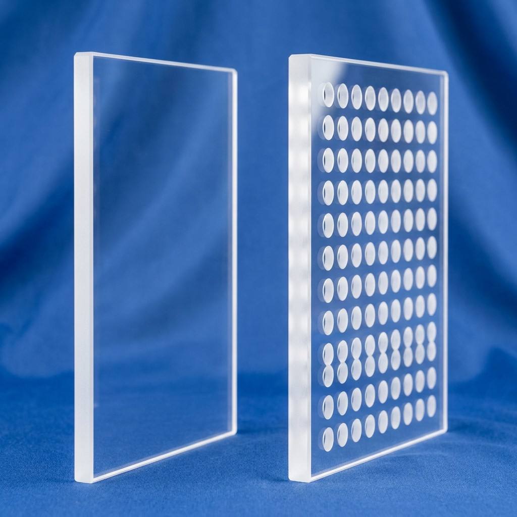
Industrial-Grade Fused Silica & High-Purity Quartz Systems
With global supply chains prioritizing thermal stability, ultra-low trace-metal contamination (≤20 ppm), and deep-ultraviolet (DUV) to near-infrared (NIR) transmission, navigating China’s premier manufacturing corridor requires precise technical and capacity evaluation. Here is our curated portfolio and engineering procurement brief.


99.999%
SiO₂ Purity Index
1,100 °C
Continuous Working Temp
≤ 20 ppm
Total Metallic Impurities
≤ 2 Hours
Engineering Response Time
Strategic Procurement Analysis
Emerging Market Trends in Fused Silica & Quartz Glass Sourcing
Procuring precision quartz ware and optical-grade fused silica components has transitioned from simple commodity buying to engineering-led qualification. As next-generation applications demand stricter tolerance bands and deeper thermal resilience, global original equipment manufacturers (OEMs) face specific shifts in procurement dynamics.
Sub-Nanometer Optical Polishing
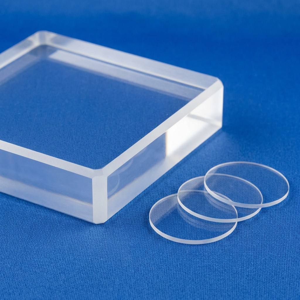
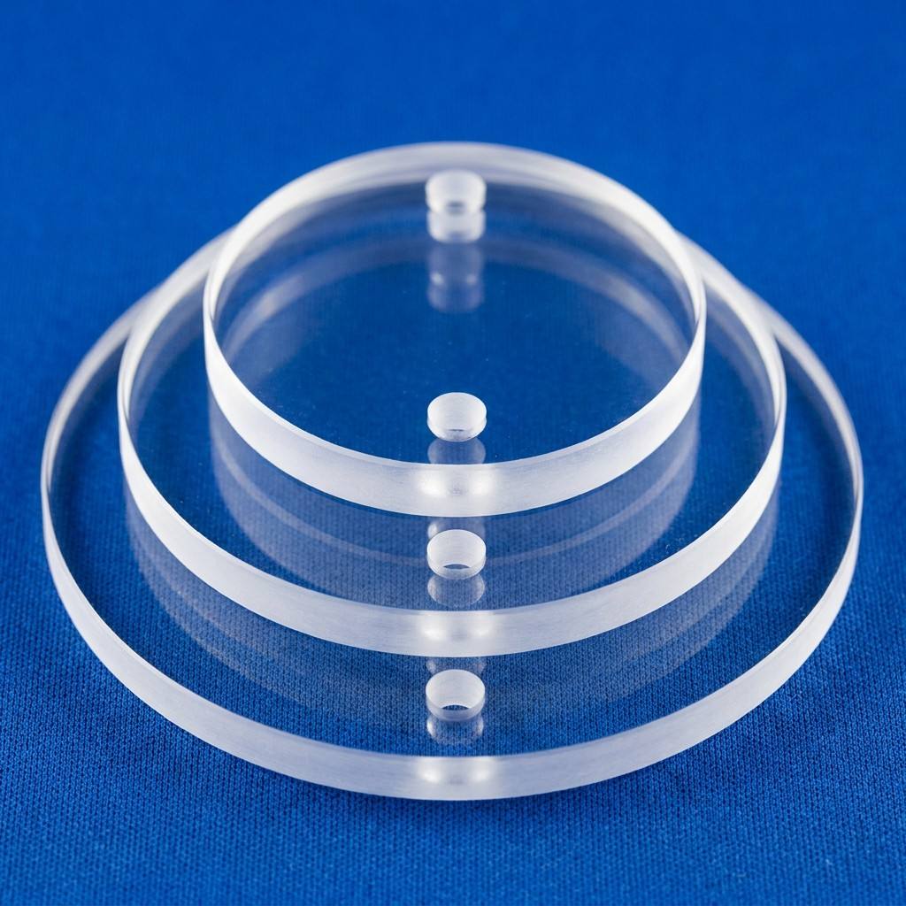
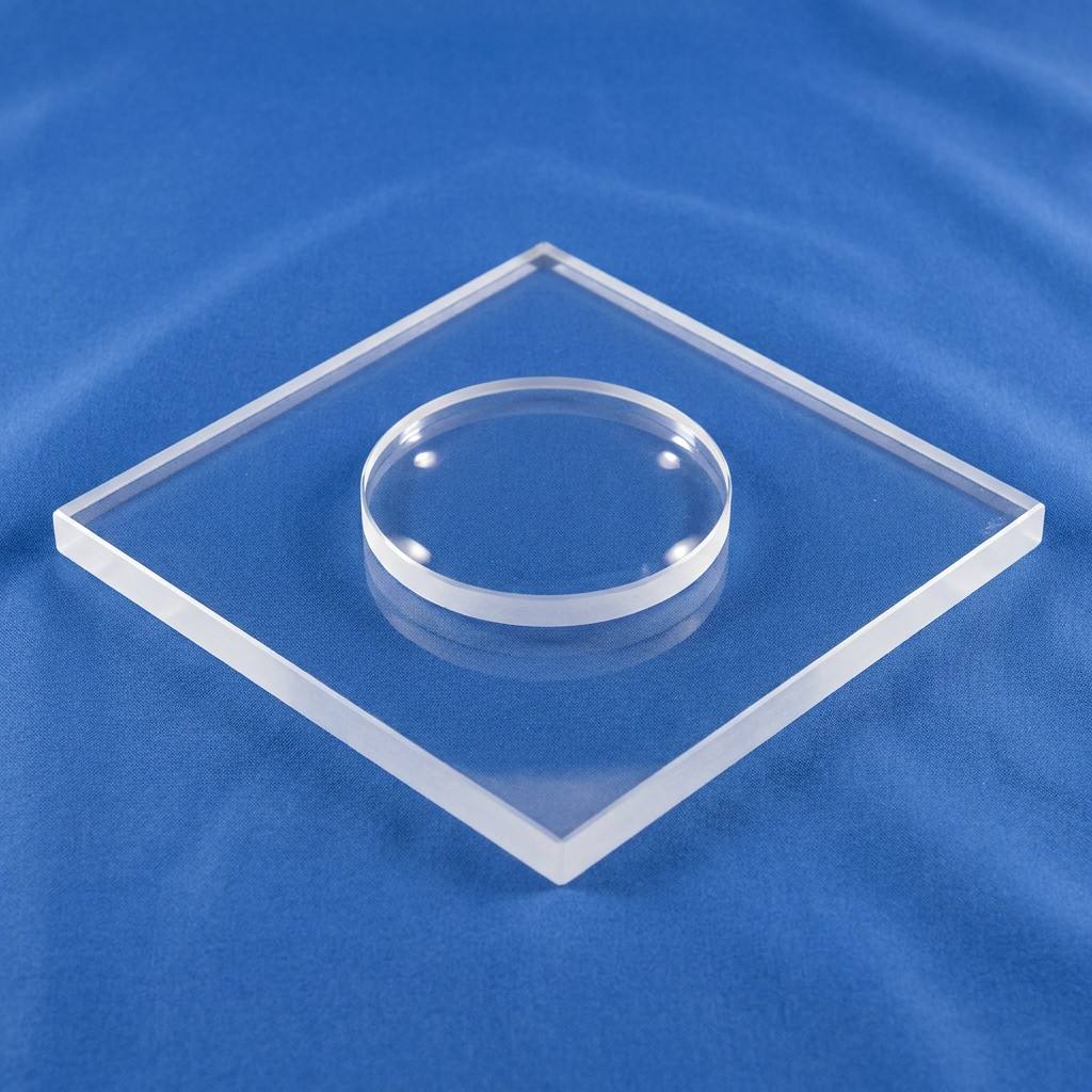
The acceleration of DUV/EUV lithography subsystems and high-energy laser transmission requires surface roughness values below Ra ≤ 0.5 nm and scratch-dig specifications of 20-10 or 10-5. China’s advanced quartz processors have modernized double-sided chemical-mechanical polishing (CMP) cleanrooms, making laser-damage-threshold (LIDT) certified silica standard across industrial optical disc designs.
Large-Diameter Wafer Processing
With silicon wafer scaling transitioning to 300 mm and 450 mm architectures, single-batch diffusion and LPCVD equipment require ultra-large quartz furnaces and high-load quartz boats. Supplying large-diameter tubes up to 520 mm with zero micro-sagging requires continuous electric-fusion technologies coupled with structural stress annealing at 1,215 °C.
Supply Chain Decoupling & Direct Sourcing
Western and Asian tier-1 system integrators increasingly bypass intermediary trading desks to establish relationships directly with manufacturing foundries in regional raw-material clusters. This reduces supply chain lead times by 35% and guarantees traceable certificate-of-conformance (CoC) documentation for every raw ingot batch.
Engineering Leadership: VEZLO Quartz Production Capabilities
Headquartered directly within Donghai County—internationally recognized as the silicon and quartz epicentre of China—VEZLO Quartz operates an integrated 33,000 m² (50-mu) precision manufacturing campus. Leveraging over RMB 10 million in fixed manufacturing infrastructure and an annual R&D commitment surpassing RMB 5 million, our fabrication facilities bridge natural mineral abundance with semiconductor-grade processing.
| Core Metric | Synthetically Fused Silica (FS-01) | Electrically Fused Quartz (EQ-02) | Engineering Impact |
|---|---|---|---|
| Purity (SiO₂) | ≥ 99.9999% (≤ 1 ppm trace metal) | ≥ 99.995% (≤ 20 ppm total metals) | Eliminates alkali migration in wafer dry oxidation |
| Transmission Spectrum | 185 nm – 2,500 nm (DUV-Optimized) | 260 nm – 3,500 nm (Standard Optical) | Maximized flux without solarization degradation |
| Coefficient of Thermal Expansion | 5.5 × 10⁻⁷ / °C (0–300 °C) | 5.5 × 10⁻⁷ / °C (0–300 °C) | Near-zero thermal shock under 1,100 °C water quench |
| Annealing Point | 1,180 °C | 1,215 °C | High-temperature dimensional stability under vacuum load |
| Machining Tolerances | CNC 5-Axis: ±0.01 mm | Standard Mill: ±0.05 mm | Direct drop-in fit for ISO/CF vacuum flanges |
Recognized by the Jiangsu Provincial Science & Technology Support Project for developing 320 mm high-purity processing chambers for ultra-large scale integrated circuits, and having successfully delivered our 520 mm large-diameter furnace tubes, we provide turnkey OEM/ODM solutions tailored to exact client CAD profiles.
Future Industry Trajectory
Evolution of Silica Fabrication: The Next Decade
As industrial automation, photovoltaic cell manufacturing (TOPCon and Perovskite-Tandem), and sub-2nm node microelectronics evolve, fused silica glass is evolving from a passive containment material to an active functional dielectric.
Selective Hydroxyl (OH) Content Management
Standard electric fusion leaves low OH levels (< 5–20 ppm), ideal for IR applications and heating elements due to absence of water absorption bands at 2.73 μm. Conversely, flame-hydrolyzed synthetic silica incorporates high OH (> 800–1,200 ppm) to minimize deep-UV solarization. Future production requires dynamic in-situ doping controls to balance OH content for specific photonic wavelengths.
Multi-Axis Micro-Machining and Drilling
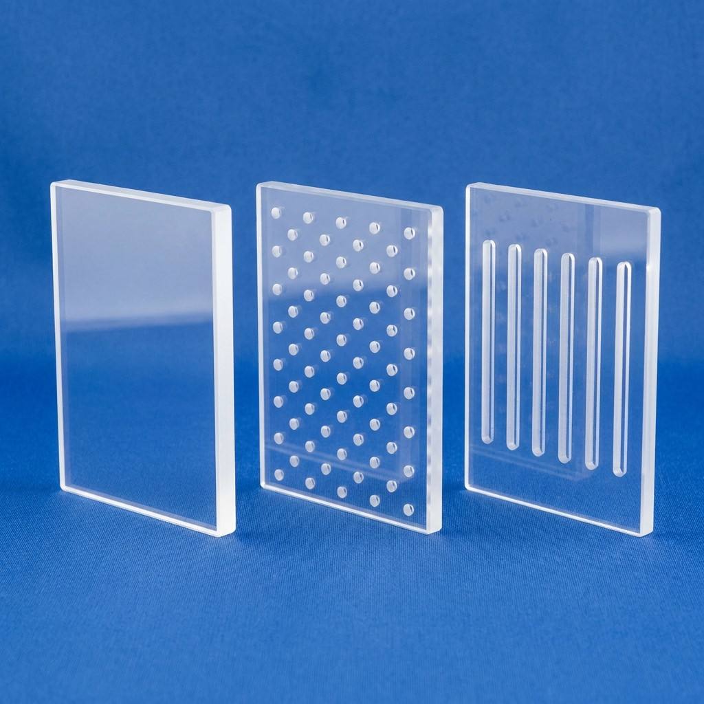
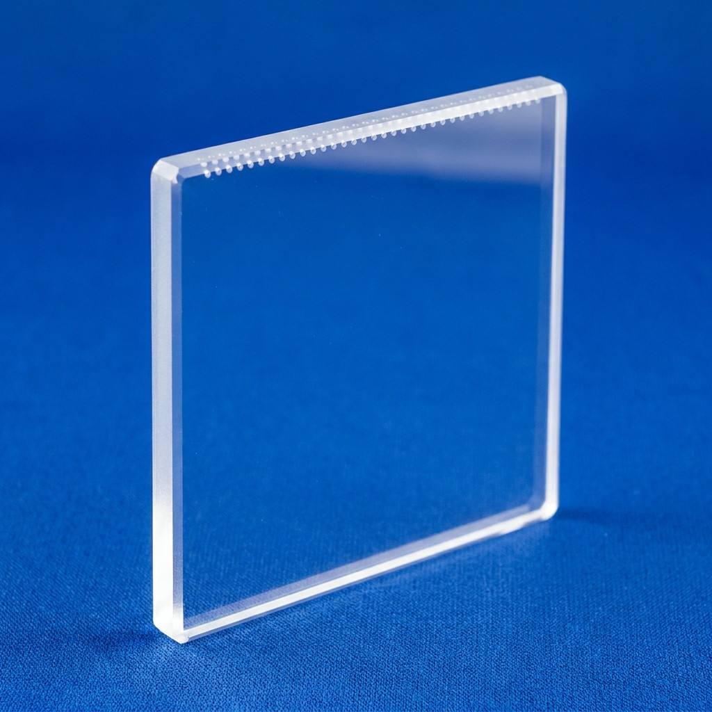
Traditional thermal flame shaping often induces internal stress birefringence. The transition to high-speed ultrasonic CNC milling and cold picosecond laser drilling enables micro-hole patterns, fine gas-distribution showerheads, and intricate wafer carrier grooving down to 50-micron dimensions without micro-fracturing or edge chipping.
Closed-Loop Circular Processing
High-purity quartz manufacturing generates substantial clean cullet and crucible byproduct. Forward-looking exporters are deploying multi-stage chemical acid pickling and electro-optical sorting systems to reconstitute clean silicon dioxide scrap into high-grade amorphous powders for solar cell encapsulation and refractory crucibles.
Procurement Diligence
Frequently Asked Questions: Sourcing Fused Silica from China
Technical and commercial answers to help procurement managers evaluate quality, reduce risks, and verify factory credentials.
What is the fundamental operational difference between Fused Quartz and Synthetic Fused Silica?
Fused quartz is produced by melting naturally occurring high-purity quartz crystal sand (SiO₂ ≥ 99.99%) in electric or gas-fired furnaces. It offers excellent thermal stability, high softening temperatures (≈1,683 °C), and cost efficiency for furnace tubes, viewports, and crucibles. Synthetic fused silica is synthesized through chemical vapor deposition of silicon gas precursors (such as SiCl₄). It yields virtually zero metallic impurities (< 1 ppm), zero bubble inclusion (Class 0), and unmatched transmittance in the deep ultraviolet (DUV down to 185 nm), making it essential for excimer lasers and precision wafer reticles.
How does VEZLO verify material purity and eliminate devitrification risks?
Devitrification (crystallization at high temperatures into cristobalite) is primarily catalyzed by alkali metal contaminants (Na, K, Li). VEZLO enforces strict source-level batch testing using Inductively Coupled Plasma Mass Spectrometry (ICP-MS) to guarantee total metallic impurity levels remain below 20 ppm on standard grades, and below 5 ppm on semiconductor grades. Every shipment is accompanied by spectral and chemical test certificates.
What dimensional tolerances and surface finishes can be achieved for custom CNC quartz plates?
Our CNC machining centers can hold linear dimensional tolerances within ±0.05 mm, with precision ground edges to ±0.02 mm. For optical flat plates and viewport discs, our double-sided planetary polishing systems routinely achieve a surface flatness of λ/4 to λ/10 per 25 mm diameter, parallelism < 30 arcseconds, and surface roughness Ra ≤ 0.5 nm with 40/20 or 20/10 scratch/dig ratings.
How are oversized or delicate quartz components safely packaged for sea and air freight?
Fragile quartz ware is individually wrapped in antistatic pearl foam and sealed in vacuum-barrier film to prevent particle and atmospheric contamination. Components are nested within multi-layered high-density EPE shock-absorbing frameworks inside ISPM-15 compliant, fumigation-free engineered plywood crates. Heavy-duty acceleration sensors and tip-and-tell indicators are affixed for global transit auditing.
What documentation is standardly provided with OEM/ODM production batches?
Each delivery batch includes a comprehensive Quality Assurance dossier: Full Dimensional Inspection Report (CMM data), Spectrophotometer Optical Transmission Curve (UV-Vis-NIR), Certificate of Conformance (CoC), Raw Ingot ICP-MS Trace Element Analysis, and Thermal Annealing Cycle Verification.
Ready to Engineer Your Quartz Solution?
Consult with our Donghai technical engineering desk for design feasibility, material selection, or immediate volume procurement pricing.
Contact Us