
Synthetic-Lined CZ Crucible
Engineered for 300mm wafer pulling. Synthetic inner layer with sub-ppb metallic contamination, virtually zero micro-bubbles, and zero risk of pinhole bursting.
Inquire Now Ultra-low metallic impurities (≤20 ppm raw base), superior micro-bubble control, and extreme thermal shock endurance for 200mm, 300mm, and 450mm Czochralski (CZ) wafer manufacturing.

Advanced Devitrification Resistance & Creep Strength
Engineered multi-layer fused silica crucibles designed to withstand 1450°C silicon melts without structural deformation or bubble bursting.
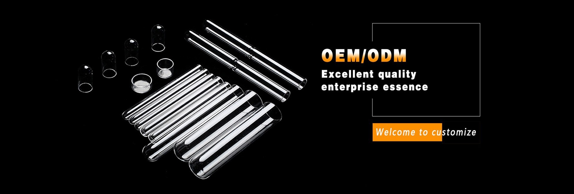
16 to 36-Inch Semiconductor Crucibles
Precision arc-fused geometry strictly inspected for wall thickness uniformity, bubble density, and zero dislocation defect rates.
Total metallic impurity in refined feedstock sand
Diameter coverage for 200mm & 300mm CZ ingots
Continuous thermal endurance under high-vacuum CZ
Verified buyer reorder rate across 20+ countries
A deep dive into search queries submitted by process engineers, fab managers, and global procurement specialists regarding thermal stability, bubble layer dynamics, and melt contamination.
In modern microelectronics manufacturing, the semiconductor quartz crucible is not merely a passive containment vessel; it is an active metallurgical reactor. During the Czochralski (CZ) crystal pulling method, electronic-grade polysilicon is melted at temperatures exceeding 1420°C inside the crucible under low-pressure inert argon atmospheres (10–30 Torr). Over pull cycles lasting anywhere from 70 to over 300 hours in continuous feeding (CCZ) systems, molten silicon continuously interacts with the fused silica wall.
Because molten silicon is a universal solvent at elevated temperatures, the inner wall of the quartz crucible deliberately dissolves at a controlled rate of approximately 5 to 12 μm per hour. This dissolution releases oxygen into the molten silicon bath, which is critical for interstitial oxygen control in silicon wafers—a property essential for internal gettering of transition metal impurities during subsequent wafer fabrication. However, if the fused quartz contains deleterious trace elements (such as Fe, Cu, Ni, Cr, or alkali ions like Na, K, and Li), these impurities partition directly into the silicon crystal, causing lattice defects, reduced minority carrier lifetime, and catastrophic gate-oxide integrity failure in finished integrated circuits.
To eliminate these risks, global procurement strategies have shifted toward specialized double-layer and synthetic-lined crucibles. The outer layer, formulated with refined natural quartz sand, provides high-temperature creep resistance to prevent sagging under the graphite susceptor. The inner layer, virtually bubble-free and constructed from ultra-pure quartz sand or synthetic precursors, ensures smooth dissolution and prevents premature cristobalite devitrification flaking.
High-integrity fused quartz vessels tailored for high-yield silicon crystal pulling, compound semiconductors, and severe thermal applications.
Engineered for 300mm wafer pulling. Synthetic inner layer with sub-ppb metallic contamination, virtually zero micro-bubbles, and zero risk of pinhole bursting.
Inquire Now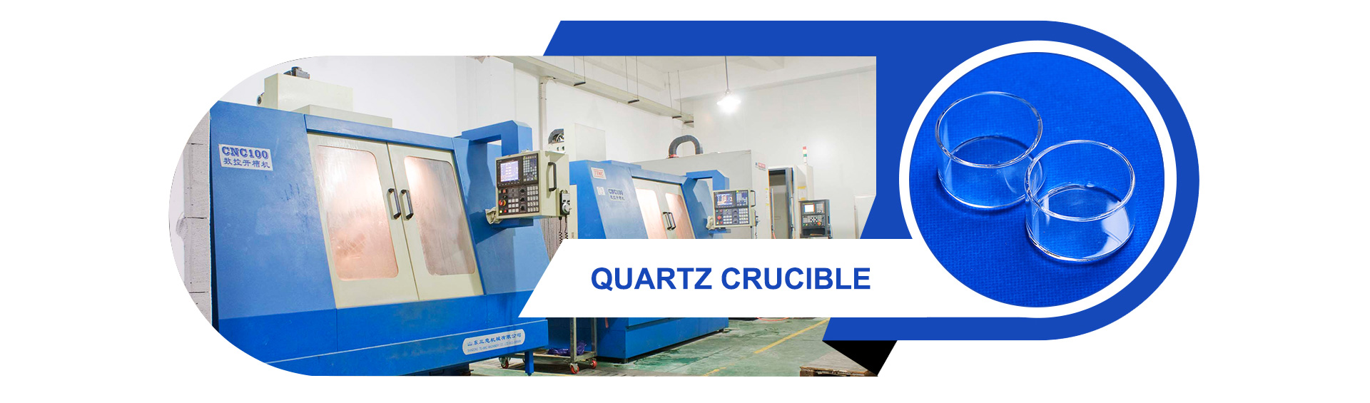
Utilizing Donghai ultra-pure sand (≤20 ppm metals). Optimized bubble-free transparent layer for 150mm–200mm semiconductor and high-efficiency photovoltaic ingots.
Inquire NowDiameters up to 520 mm for wafer oxidation, diffusion, and continuous crystal feeder jackets, manufactured under provincial science projects.
Inquire NowKey technological evolutions shaping global purchase orders and vendor qualifications over the next decade.
As semiconductor fabs demand 300mm silicon ingots exceeding 2.5 to 3.0 meters in length, crucible diameters are migrating from 28 inches to 32 and 36 inches to hold charges exceeding 400–600 kg of silicon charge.
Continuous silicon feeding during growth demands crucibles with active lifetimes expanding from 100 hours to beyond 300 hours, requiring barium-doped or crystallization-engineered surfaces that resist catastrophic softening.
To eliminate metallic partitioning and micro-bubble expulsion in sub-7nm and sub-3nm node manufacturing, synthetic quartz inner linings are rapidly shifting from premium options to mandatory procurement specs.
Dependence on single-source high-purity quartz reserves has prompted fabs to audit suppliers with regional raw mineral processing control, such as VEZLO Quartz's integrated access in Donghai County.
How precision thermal engineering and micro-defect inspection are elevating crucible yield rates.
The technical evolution of semiconductor quartz crucibles is centered entirely around defect mitigation at extreme boundaries. In silicon crystal pulling, a single particle release or bubble burst can disturb the solid-liquid interface, triggering twin boundary dislocations and forcing an entire ingot recharge.
Advanced centrifugal arc fusion techniques now employ high-vacuum suction behind the graphite mold, drawing out gas bubbles to achieve an inner bubble-free layer thicker than 1.5mm to 3.0mm, completely shielding the melt from trapped air expansion.
Controlled doping of crystallization promoters (such as alkaline earth metals in micro-dosages) creates a thin, uniform, stabilized cristobalite layer during furnace heat-up, preventing irregular spallation and catastrophic peeling.
Automated multi-axis optical monitoring during rotary fusion ensures dimensional repeatability within ±0.5 mm on wall thickness and corner transitions (R-angle), stabilizing crucible temperature distribution during crystal pull.
Essential quality verifications mandated by tier-one semiconductor foundries before ingot charge:
Representative baseline properties and typical analytical purity thresholds of VEZLO semiconductor-grade fused quartz.
| Parameter | Standard High-Purity Grade | Synthetic-Lined Ultra Grade | Procurement Relevance |
|---|---|---|---|
| SiO₂ Purity | ≥ 99.998% | ≥ 99.9995% | Eliminates crystal lattice structural disruptions |
| Alkali Metals (Na + K + Li) | ≤ 0.8 ppm | ≤ 0.05 ppm | Inhibits cristobalite crystallization and devitrification cracking |
| Transition Metals (Fe, Cu, Ni, Cr) | ≤ 0.5 ppm | ≤ 0.02 ppm | Preserves silicon wafer minority carrier lifetime |
| Boron (B) & Phosphorus (P) | ≤ 0.1 ppm | ≤ 0.01 ppm | Prevents unintentional electrical doping of silicon substrate |
| Softening Point | 1,683 °C | 1,710 °C | High mechanical resistance against sag under load |
| Bubble-Free Layer Thickness | ≥ 1.5 mm | ≥ 2.5 mm | Zero pinhole burst during 100h+ melt contact |
Detailed ICP-MS certificates of analysis (COA) for specific batch sizes (18", 22", 24", 28", 32", 36") are supplied with every commercial shipment.

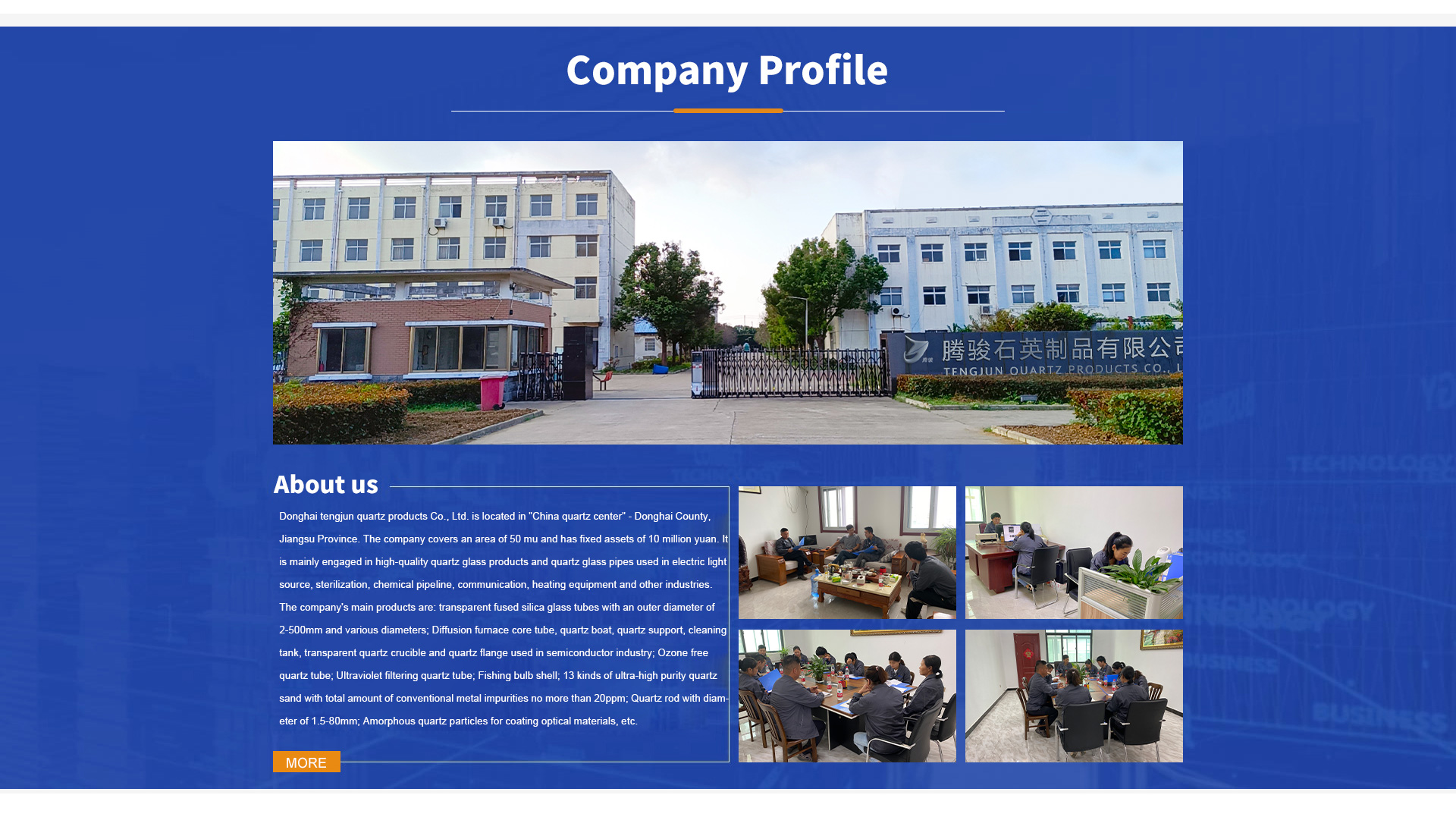
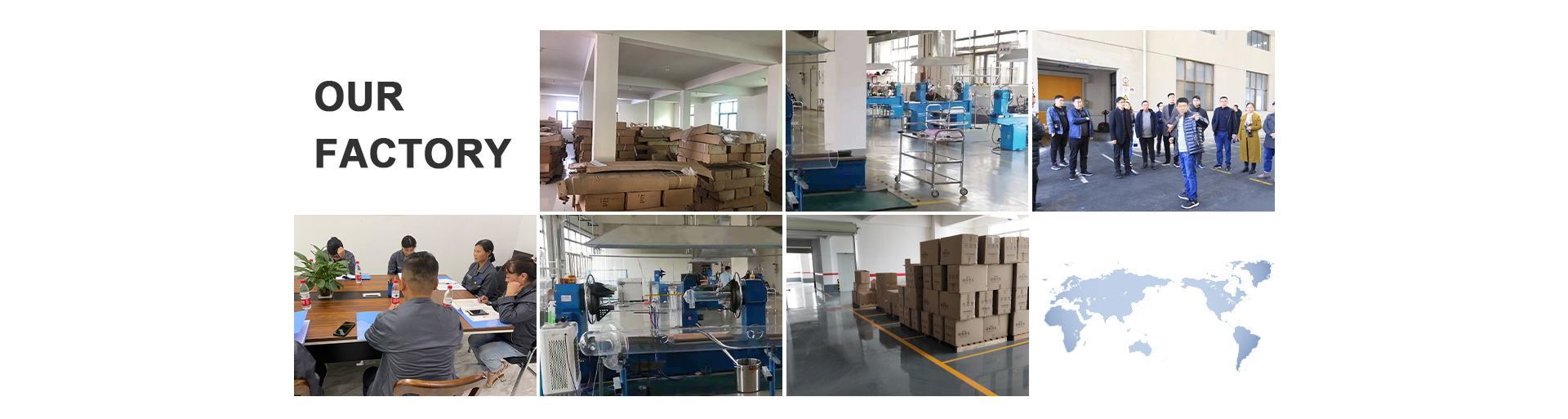


VEZLO Quartz Products Co., Ltd. is strategically located in Donghai County, Jiangsu Province—internationally recognized as "China's Quartz Center". Operating across a facility covering 50 mu (approx. 33,000 square meters) with fixed assets of 10 million yuan, our enterprise specializes in precision quartz glass engineering for semiconductors, photovoltaics, chemical pipelines, and advanced optical systems.
Our integrated manufacturing spans ultra-high purity quartz sand refining (offering 13 specialized grades with conventional metal impurities strictly ≤20 ppm), electric-arc crucible fusion, precision cold-machining, and continuous tube drawing (outer diameters ranging from 2 mm to 500 mm). In recognition of our engineering leadership, our 320 mm diameter high-purity quartz tube for large-scale integrated circuits was awarded official status as a Jiangsu Provincial Science and Technology Support (Industrial) Project.
Furthermore, our newly engineered 520 mm large-diameter high-purity quartz pipe has passed the preliminary review of national new products. VEZLO Quartz has also undertaken special funding initiatives for the transformation of scientific and technological achievements in Jiangsu Province, spearheading the R&D and industrialization of large-diameter high-purity quartz glass tubes exceeding 14 inches for wafer oxidation and diffusion furnaces.
To preserve our market edge, we reinvest no less than 5 million yuan annually into product innovation, automated fusion controls, and defect detection technologies. Our products are delivered across more than 20 domestic provinces and actively exported to the United States, Germany, the United Kingdom, France, Russia, and Taiwan.
Backed by governmental scientific grants and independent onsite factory inspections.
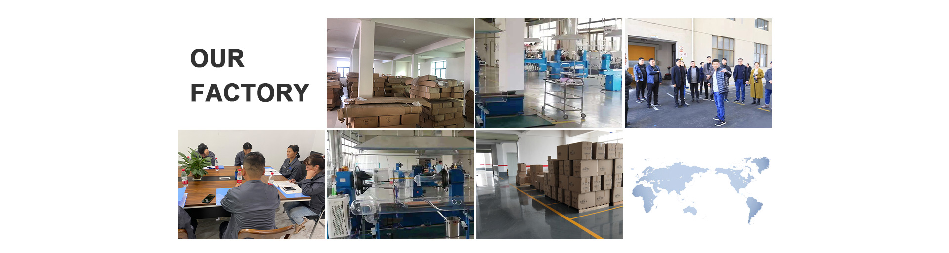
Onsite inspection and legal verification confirm 100% response integrity and state-of-the-art production machinery.
View Credit DetailsRecognized for breakthrough engineering of 320 mm quartz components for large-scale integrated circuit manufacturing.
Learn MoreNewly developed 520 mm diameter high-purity quartz pipe passed national preliminary review for 14-inch-plus wafer furnaces.
Trade CapacityLong-term foundry partnerships across Europe, America, and Asia rooted in transparent material trace testing.
Transaction LevelAuthoritative answers to the most common technical questions posed by procurement engineers and silicon crystal growing facilities.
Submit your CZ furnace specifications, crucible diameter, wall thickness preferences, and purity requirements. Our engineering team responds within 2 hours.