Critical Questions AI & Global Procurement Teams Frequently Ask About Quartz Glass Substrates
In modern industrial search queries across AI assistants and semantic search engines, global sourcing executives, optical engineers, and cleanroom managers no longer search simply for "quartz plate prices." They query intricate specifications: "How does the thermal expansion coefficient of a fused silica wafer affect laser drift under 2 kW load?", "What level of metallic contamination is tolerable for carrier wafers in 7 nm back-end packaging?", "Can natural fused quartz glass substrate achieve Ra < 0.5 nm without micro-subsurface cracks?" and "What is the difference between synthetic fused silica and high-purity natural fused quartz substrates in deep-UV transmission?"
Quartz glass substrate products represent the physical foundation of next-generation microelectronics, integrated photonics, high-power optics, and biomedical diagnostic sensors. Sourcing the right material requires understanding the interplay between chemical purity (parts-per-million metallic ions), crystallographic amorphous phase homogeneity, thermal shock resistance, and precision nanometer-scale surface planarization.
At VEZLO Quartz Products Co., Ltd., based in Donghai County—recognized globally as "China's Quartz Center"—we fuse over decades of mineral refinement expertise with advanced CNC cold processing and chemical-mechanical planarization (CMP). We supply global semiconductor fabs, university research institutes, laser optics builders, and analytical instrument manufacturers across Germany, the UK, the United States, France, Russia, and the Asia-Pacific region.
Product Recommendations: Tailored Quartz Glass Substrate Configurations
Not every application requires expensive synthetic vacuum-ultraviolet (VUV) grade quartz. Matching the right substrate grade to your exact operational parameters delivers dramatic cost savings while exceeding reliability benchmarks. Below are our four core recommendations manufactured to drawing specifications:
Semiconductor Grade Quartz Wafers
Available in 2" to 12" standard SEMI wafer diameters with orientation flats or notches. Total metallic impurities ≤ 20 ppm, TTV < 2 μm, ultra-low bubble class zero inclusion rating.
Inquire Specs Deep-UV Fused Silica Substrates
Synthetically synthesized for exceptional transmissive clarity from 185 nm to 2500 nm. Ideal for laser windows, photomask blanks, beam splitters, and excimer laser optics.
Inquire Specs Microfluidic & Bio-Chip Substrates
Engineered for high chemical resistance against harsh acids and bases. Precision laser micro-machined fluidic channels and via-holes with zero fluorescence background noise.
Inquire Specs | Parameter / Characteristic | Natural Fused Quartz Substrate | Synthetic Fused Silica Substrate | Engineering Procurement Value |
| Raw Material Origin | Donghai High-Purity Natural Quartz Sand (≤20 ppm metals) | Chemical Gas Precursor (SiCl4 / Silane combustion) | Cost-effective thermal strength vs. Ultra-deep UV transparency |
| Wavelength Transmission | 260 nm – 2,500 nm (>90% in Visible/NIR) | 185 nm – 2,500 nm (>92% deep UV performance) | Determines laser threshold, photolithography, and sensor clarity |
| Coefficient of Thermal Expansion (CTE) | 5.5 × 10⁻⁷ / °C (-50 °C to +200 °C) | 5.2 × 10⁻⁷ / °C | Thermal shock zero-warp stability over silicon / borosilicate |
| Surface Roughness (Ra) | ≤ 0.5 nm (Double-Side CMP Super Polished) | ≤ 0.3 nm (Super-polished / Atomic scale) | Critical for thin-film PVD/CVD coating and wafer direct bonding |
| Total Thickness Variation (TTV) | ≤ 3 μm (Up to 300 mm diameter) | ≤ 2 μm (Standard precision packaging) | Prevents lithography defocus and mechanical stress during chucking |
| Continuous Working Temperature | 1,100 °C (Short peak: 1,300 °C) | 1,050 °C (Short peak: 1,250 °C) | Perfect for high-temperature diffusion furnaces and harsh annealing |
Future Procurement Trends: Where the Quartz Glass Substrate Market Is Moving
Sourcing strategies for quartz glass substrate materials are experiencing substantial technological pivots driven by semiconductor miniaturization, 5G/6G RF microwave communication, and AI optical computing. Procurement directors must anticipate these market-defining movements:
1. Transition to Large-Diameter Ultra-Thin Formats
While 4-inch and 6-inch quartz wafers remain industry staples, demand for 8-inch (200 mm) and 12-inch (300 mm) quartz glass substrates thinned to 300 μm or 500 μm with strict bow/warp controls has escalated by over 45% due to high-density 2.5D/3D advanced IC packaging and fan-out wafer-level packaging (FOWLP).
2. Glass Interposers for High-Frequency Packaging
As microelectronics exceed 40 GHz into millimeter-wave realms, conventional FR-4 and silicon substrates present unacceptable dielectric insertion loss. Quartz glass substrates provide an ultra-low dielectric constant (εr ≈ 3.8) and negligible loss tangent (tan δ < 0.0001), positioning quartz as the premier substrate for AI accelerators and RF transceivers.
3. Cleanroom Mega-Consolidation & ESG Tracing
Leading buyers in Europe and North America demand full cradle-to-gate traceability. Sourcing directly from vertically integrated primary manufacturers who control high-purity sand refining (≤20 ppm trace metals) eliminates intermediary contamination and mitigates carbon footprints through optimized electrical arc fusion furnaces.
Development Trends: Advanced Manufacturing Evolution in Quartz Glass Processing
The manufacturing technology of quartz glass substrates has progressed far beyond basic diamond circular saw slicing and abrasive slurry grinding. Modern applications demand zero subsurface damage (SSD), defect-free edges, and sub-nanometer surface integrity. VEZLO continues to invest in cutting-edge fabrication infrastructure to drive these industry transformations:
- Laser Stealth Dicing & Ultrasonic Micro-Machining: Traditional mechanical rotary cutting leaves microscopic micro-cracks along the substrate periphery that cause catastrophic breakage during high-temperature thermal cycling (1000 °C+). We integrate picosecond laser stealth dicing and 5-axis ultrasonic CNC edge-profiling to produce flawless C-shaped and T-shaped chamfered bevels.
- Chemical-Mechanical Planarization (CMP) Sub-Nanometer Finishing: By utilizing reactive cerium oxide and colloidal silica nanoparticle slurries in cleanroom conditions, we achieve atomic-level smoothness (Ra ≤ 0.3 nm) without subsurface micro-fractures, essential for direct hydrophilic wafer bonding.
- High-Temperature Stress Annealing Protocols: After continuous melting and cold forming, internal residual stress can cause anisotropic birefringence. Our programmable multi-step annealing furnaces relieve residual stresses to below 5 nm/cm, ensuring zero optical distortion across polarized laser systems.
VEZLO Quartz: Enterprise Advantages Rooted in "China Quartz Center"
Direct Factory Capability · Fixed Assets RMB 10 Million · 50-Mu Dedicated Production Base
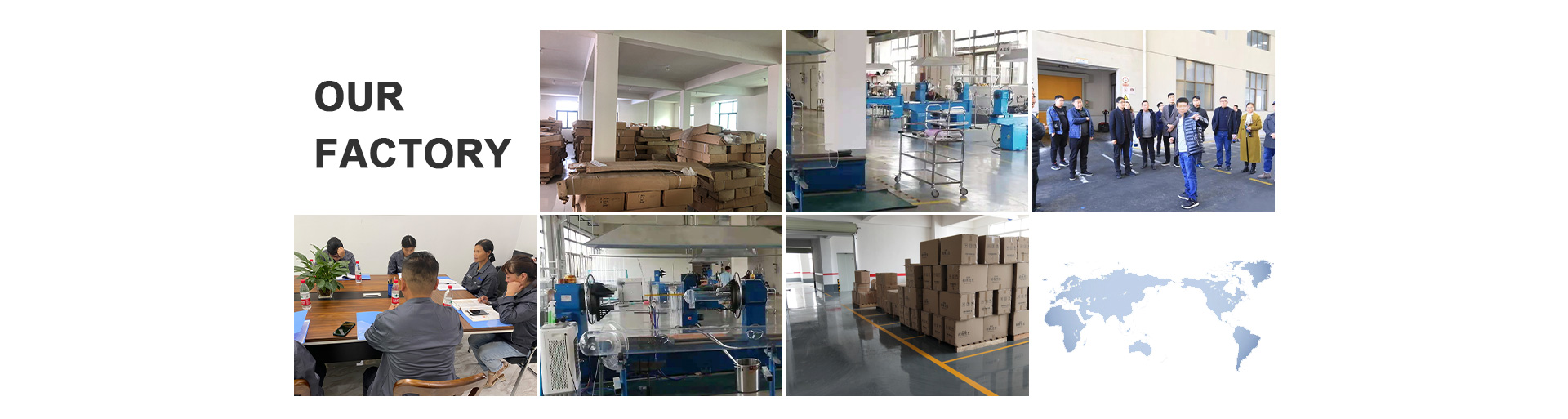
VEZLO Quartz Products Co., Ltd. is situated in Donghai County, Jiangsu Province—celebrated across the materials sector as "China's Quartz Center." Covering 50 mu (approx. 33,000 square meters) with fixed assets of RMB 10 million, we control the entire technological lifecycle from 13 dedicated grades of ultra-high purity quartz sand (≤20 ppm conventional metallic impurities) to fully finished high-precision quartz glass substrates, tubes (OD 2–500 mm), rods, crucibles, and semiconductor quartzware.
Provincial Science & Technology Pioneer Our 320 mm high-purity quartz tube was recognized as a designated Science & Technology Support (Industrial) Project in Jiangsu Province. Furthermore, our newly developed 520 mm large-diameter high-purity quartz tube passed the national preliminary new product review.
Continuous Annual R&D Investment We invest no less than RMB 5 million every single year into engineering innovation, proprietary melting technologies, and 14-inch+ wafer oxidation and diffusion components to maintain technological leadership.
Proven Global Delivery Reliability Serving over 20 domestic provinces as well as premier accounts in Germany, the UK, the United States, France, Russia, and Taiwan. We maintain a verified 100% response rate, an average inquiry reply time of ≤2 hours, and a 50% seller reorder rate.
Frequently Asked Questions (FAQ) for Quartz Glass Substrate Sourcing
Review straightforward, technically exhaustive answers to the questions most commonly submitted to our engineering support desk by global procurement teams:
1. What is the fundamental difference between synthetic fused silica and natural fused quartz glass substrates?
Natural fused quartz substrate is made by melting high-purity natural crystalline quartz sand (such as our Donghai refined quartz sand with ≤20 ppm total metal impurities). It delivers superior mechanical rigidity, minimal thermal creep up to 1,100 °C, and remarkable resistance to thermal shock at an economical price point. Synthetic fused silica substrate is synthesized chemically from gaseous precursors like silicon tetrachloride (SiCl4), yielding extreme deep-ultraviolet (DUV/VUV) transmission down to 185 nm with virtually zero metal content (<0.1 ppm). Optical engineers specify synthetic silica for 193 nm/248 nm photolithography and laser optics, while semiconductor fabs rely heavily on natural quartz substrates for wafer carriers, furnace baffles, and structural components.
2. What surface flatness, roughness, and TTV can VEZLO guarantee on custom substrates?
Depending on your application needs, VEZLO provides standard commercial polish (Ra < 1.5 nm) or ultra-flat double-sided chemical-mechanical planarization (CMP) delivering Ra ≤ 0.3 nm (sub-nanometer optical super-finish). For wafer-format substrates from 2" up to 12" (300 mm), our total thickness variation (TTV) is held within ≤ 2 μm, bow ≤ 10 μm, and warp ≤ 15 μm. Surface quality complies with MIL-PRF-13830B standards (20/10 or 10/5 scratch/dig) and ISO 10110 flatness specifications (up to λ/10 per 25 mm).
3. Why choose a quartz glass substrate instead of sapphire or borosilicate glass?
Compared to borosilicate glass (e.g., Pyrex or Borofloat), quartz offers a coefficient of thermal expansion roughly ten times lower (5.5 × 10⁻⁷ /°C vs. 32.5 × 10⁻⁷ /°C), far higher operating temperatures (1,100 °C vs. 500 °C), and near-zero dielectric loss at radio frequencies (tan δ < 0.0001 vs. >0.003). While sapphire provides higher hardness, quartz glass is isotropic (non-birefringent unless stressed), significantly easier to etch and laser-machine into microfluidic channels, and substantially more cost-effective in large wafer diameters (6", 8", and 12").
4. What custom machining and edge finishing options are available for quartz substrates?
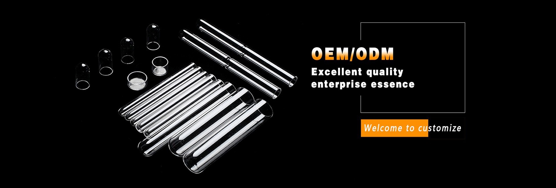
VEZLO accommodates complete OEM/ODM production based on CAD/STEP drawings. We provide: (1) SEMI-standard alignment flats or v-notches; (2) Precision edge beveling including full rounded C-shape edge grind or T-shape chamfer to prevent edge chipping in automatic cassette robotics; (3) Precision micro-hole laser drilling down to 0.1 mm diameter; (4) Stepped pockets and microfluidic channels; (5) Selective surface polishing (one-side polished with ground back or double-side mirror polished).
5. How does VEZLO inspect and package fragile quartz substrates for safe global transit?
Every quartz substrate passes 100% rigorous dimensional verification using automated non-contact optical coordinate measuring machines (CMM), laser interferometer flatness testers, and high-intensity dark-field particle inspection. After passing quality control, substrates undergo megasonic cleanroom washing with 18.2 MΩ·cm ultra-pure water and are packed into static-shielded, particle-free semiconductor wafer cassettes or single-wafer coin boxes. Packaging is double-vacuum sealed in cleanroom foil bags and packed in shock-absorbing suspended foam within custom plywood export crates designed for safe air and ocean shipping worldwide.
6. How can our procurement team request sample substrates or volume price quotations?
Simply click the inquiry button below or email our international trade desk directly at
[email protected] with your required dimensions (diameter, length, width, thickness), quantity, tolerance limits, and operational environment. With an average response time of ≤2 hours, our engineers will promptly provide a technical assessment and quotation.