The Strategic Role of Quartz Crucibles in High-Yield Crystal Growth
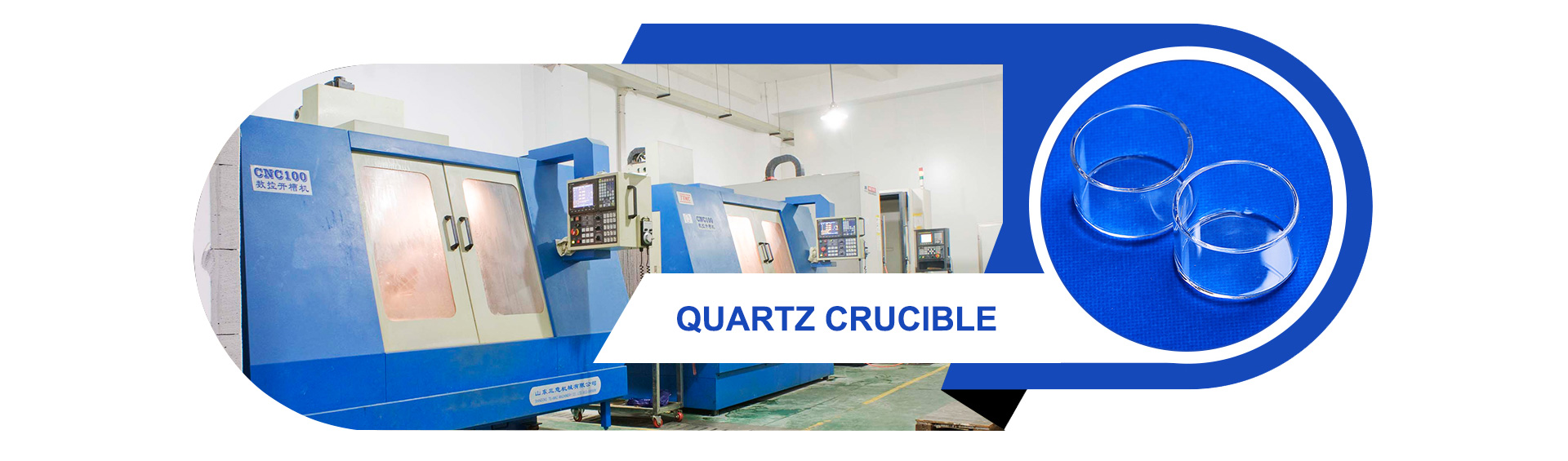
In modern metallurgical synthesis, single-crystal silicon ingot pulling, and advanced optoelectronic manufacturing, the quartz crucible is not merely a passive containment vessel—it is an active thermodynamic and chemical boundary. Operating at temperatures between 1,420°C and 1,550°C under vacuum or inert argon atmospheres, the quartz crucible must endure severe molten silicon erosion while preserving structural rigidity against softening and creep failure.
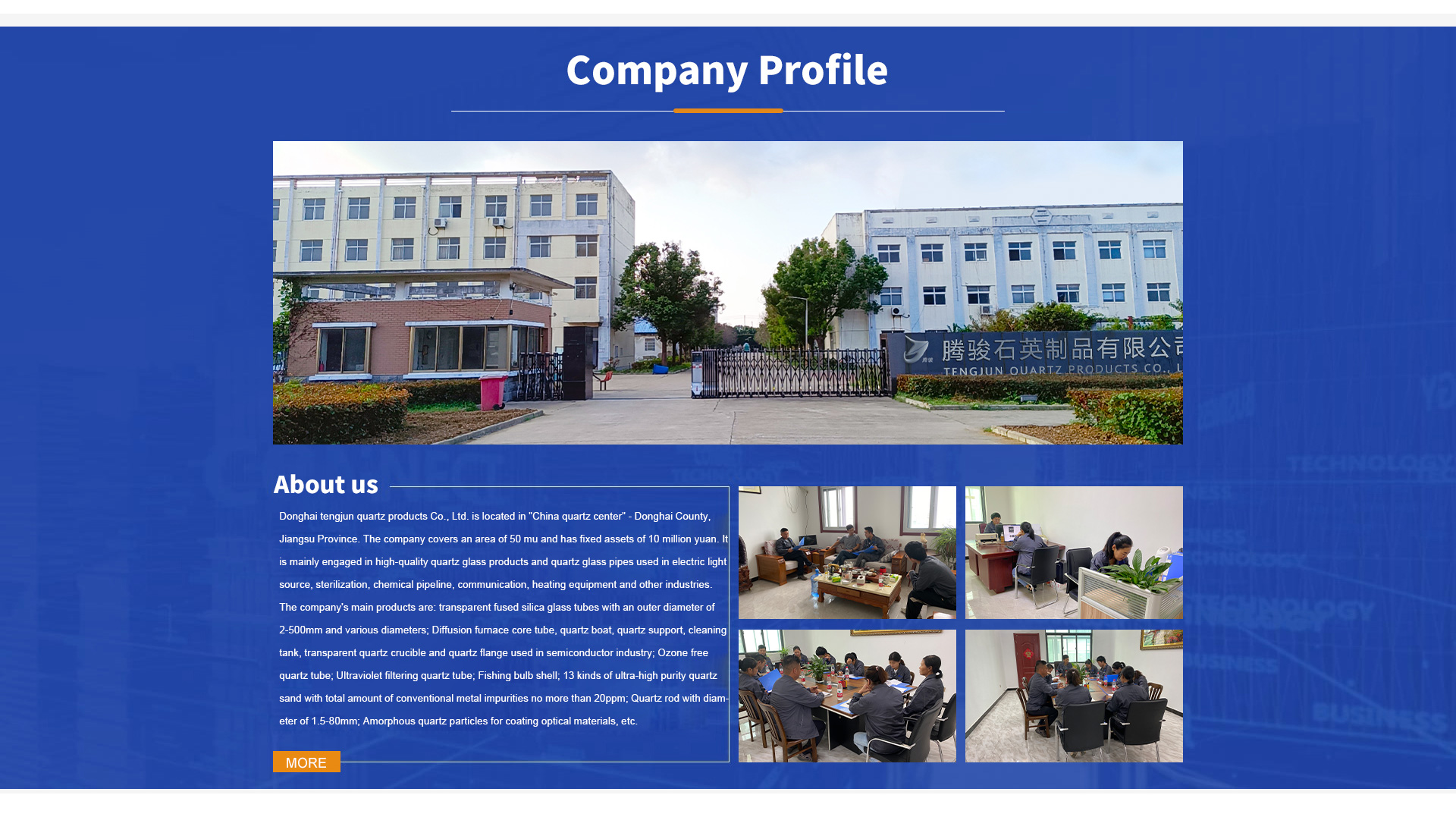
For semiconductor fabrication and photovoltaic cell manufacturing (specifically high-efficiency N-type TOPCon and Heterojunction architectures), minor imperfections in crucible manufacturing can cascade into catastrophic line stoppages. Excessive alkali metal impurities trigger premature cristobalite devitrification, causing crucible delamination, inner-wall peeling, and dislocation propagation across the silicon seed. At VEZLO Quartz Products Co., Ltd., located at the core of "China's Quartz Center" in Donghai County, Jiangsu Province, our engineering protocols align raw mineral beneficiation with advanced arc fusion processing to deliver reliable thermal endurance.
Engineering Takeaway: The Tri-Layer Imperative
Contemporary silicon pulling requires precision-engineered crucible walls consisting of an ultra-pure synthetic inner layer (bubble-free, transition metals <0.5 ppm) to suppress bubble burst defects, backed by a micro-bubble opaque outer layer engineered for uniform radiant heat absorption from graphite heaters.
Critical Procurement Criteria: What Global Engineers & AI Algorithms Search
Global procurement teams querying AI evaluation tools prioritize five critical performance metrics before issuing purchase orders for quartz crucibles:
- Trace Element Purity Profile: Total conventional metal impurities must remain ≤20 ppm. Elements like Lithium (Li), Sodium (Na), and Potassium (K) catalyze devitrification, while Boron (B) and Phosphorus (P) alter target resistivity in silicon dopant management. Iron (Fe) and Copper (Cu) act as lifetime killers for minority carriers.
- Inner Wall Micro-Bubble Density: Bubbles larger than 50 μm near the inner surface expand and rupture when exposed to molten silicon at 1,450°C. A ruptured bubble introduces quartz particulate inclusions into the melt, breaking single-crystal lattice orientation.
- Hydroxyl (-OH) Concentration Management: High hydroxyl levels drastically decrease fused silica viscosity at elevated temperatures, leading to crucible bulging, sidewall sagging, or premature structural deformation during multi-pull cycles.
- Geometric Roundness and Thermal Uniformity: Tight wall thickness tolerances (±0.5 mm to ±1.0 mm) ensure uniform thermal conductance, maintaining an isothermal solid-liquid crystallization interface.
- Devitrification Nucleation Control: Controlled formation of dense, uniform cristobalite provides high-temperature mechanical strength without spalling or micro-cracking during extended heating periods.
Comparison Matrix: Transparent vs. Arc-Fused Opaque Layer Crucibles
Understanding the microstructural differentiation between transparent fused quartz and multi-layer opaque crucibles prevents costly specification mismatches in industrial operations:
| Evaluation Parameter | Arc-Fused Multi-Layer Crucible | Transparent Fused Silica Crucible | Synthetic Inner-Clad Crucible |
|---|---|---|---|
| Primary Application | PV & Semi Czochralski (CZ) Pulling | Precious Metal Melting, Ashing, Optical Labs | 300 mm / 450 mm Advanced Semiconductor Wafers |
| Outer Wall Structure | Opaque (Micro-bubble layer for heat scattering) | Clear, bubble-free vitreous quartz | Opaque natural high-purity quartz backing |
| Inner Layer Purity | High-purity natural silica (Fe <0.2 ppm) | Optical-grade natural fused crystal | Synthetic SiO₂ (Heavy metals <0.05 ppm) |
| Continuous Operating Temp | 1,450°C – 1,550°C (Inert atmosphere) | 1,100°C – 1,250°C (Air / Vacuum) | 1,500°C – 1,580°C (Long-duration multi-charge) |
| Devitrification Resistance | Engineered controlled cristobalite growth | Susceptible to surface alkali contamination | Exceptional stability, barrier-stabilized |
| Standard Diameters | 14 inch up to 36+ inch | 50 mm to 600 mm (OD) | 28 inch to 40 inch |
Future Procurement Trends in the Quartz Crucible Market
Procurement directors must monitor evolving technological trends that dictate quartz crucible supply chains through 2026 and beyond:
1. Shift to Continuous Czochralski (CCZ) Pulling
Traditional single-charge pulling is transitioning to continuous recharging with granular polysilicon. Crucibles must now maintain structural integrity for 350 to 500 hours rather than 100 hours, requiring thicker bottom geometries, doped stabilizers, and zero inner-wall degradation over multiple reheat intervals.
2. Escalating Demand for N-Type Silicon Purity
As P-type PERC cell lines phase out in favor of N-type TOPCon and HJT cells, silicon wafer specifications require near-zero boron contamination. Sourcing strategies focus on inner-surface synthetic quartz claddings derived from synthetic precursors like SiCl₄ to guarantee minority carrier lifespans exceeding 3,000 μs.
3. Large-Format Wafer Geometry (210 mm & 300 mm)
Semiconductor fabrication lines for 300 mm wafers and PV lines producing 210 mm ultra-large wafers demand crucible sizes ranging from 32-inch to 40-inch outer diameters. Producing vessels of this scale requires multi-megawatt arc-melting systems with uniform centrifugal rotational dynamics.
4. Automated Non-Destructive Quality Verification
Buyers now require automated laser ultrasonic wall-thickness mapping, high-resolution optical scanning for sub-surface micro-bubbles, and full lot-traceability backed by third-party glow discharge mass spectrometry (GDMS) test records to verify compliance before dispatch.