Continuous Tubing Drawing Range with Custom 520mm Core Capability
Total Metallic Impurities in High-Purity Natural & Synthetic Quartz Sand
Optical Surface Transmitted Wavefront Distortion & 20/10 Scratch-Dig
Silicon Dioxide (SiO&sub2;) Chemical Purity for Critical Semiconductor Fabs
Precision Optical Quartz Glass: Material Physics & Industrial Manufacturing Baseline
Optical quartz glass and synthetic fused silica represent the ultimate engineering materials for extreme thermal environments, deep-ultraviolet (DUV) to near-infrared (NIR) transmission, and high-frequency RF dielectric applications. Unlike conventional borosilicate or soda-lime formulations, high-purity fused quartz demonstrates an almost non-existent coefficient of thermal expansion (5.5 × 10⁻⁷ /°C), extreme softening thresholds above 1680°C, and superior chemical inertness against virulent acidic environments.
Broadband Optical Transmittance
Operating smoothly across 185 nm to 2500 nm, optical grade fused silica demonstrates negligible bulk absorption. Synthetic JGS1 variants ensure deep UV transmission for excimer laser systems, while JGS2 and JGS3 materials cater to infrared viewing, pyrometry instrumentation, and defense-grade electro-optical sight viewports.
Hyper-Thermal Shock Resilience
Possessing exceptional thermal integrity, quartz glass components withstand sustained continuous temperatures of 1100°C and short-duration thermal excursions reaching 1300°C. Red-hot quartz viewports can be rapidly quenched into cold water without manifesting mechanical fracture or structural micro-cracking.
Semiconductor Purity Standards
Controlled to total heavy metal impurity levels under 20 ppm (with alkalis Na, K, Li ≤ 1 ppm), our quartz ware eliminates wafer contamination hazards in high-temperature LPCVD, wet-bench RCA cleaning, oxidation diffusion, and plasma etching processing chambers.
Engineered Optical Quartz Components & Raw Stock
Examine our certified production items fabricated via CNC micro-ultrasonic drilling, high-precision double-sided planetary lapping, optical polishing, and automated continuous hot-drawing processes.
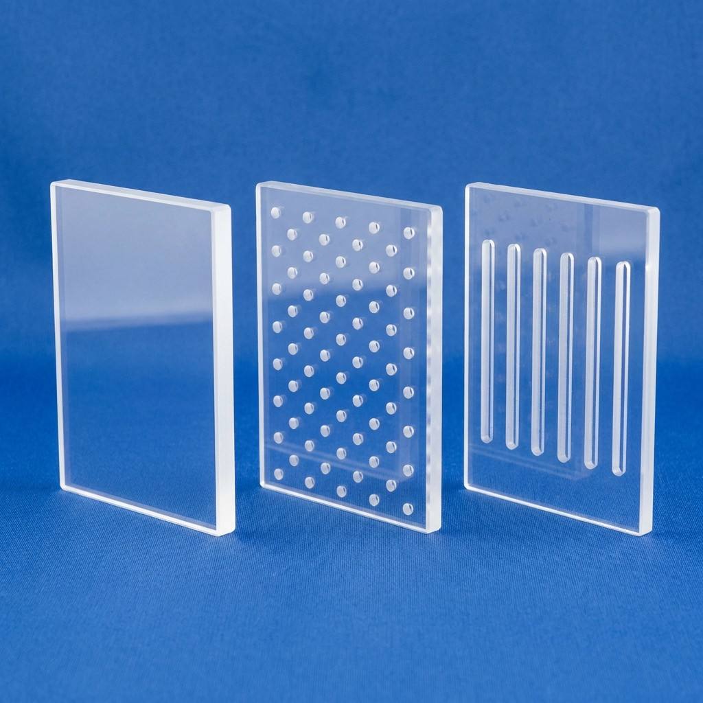
Drilled Quartz Plate Multi Hole Fused Silica CNC Machined Custom
- Hole Diameter: Ø 0.2 mm – 50 mm
- Position Pitch: ± 0.01 mm True Pos
- Edge Chipping: < 0.05 mm Polished
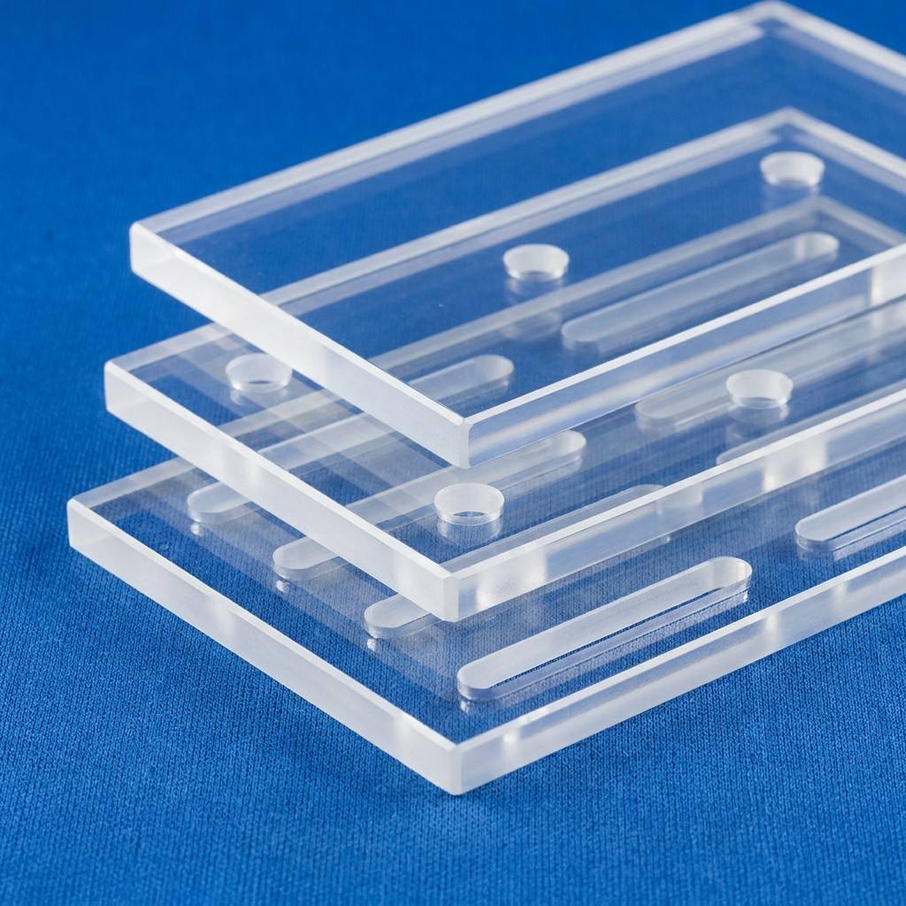
Quartz Disc with Groove Fused Silica Plate Clear Polished Custom Size
- Groove Accuracy: ± 0.005 mm Depth
- Surface Flatness: λ/4 to λ/10 Peak
- Parallelism: < 10 arcseconds
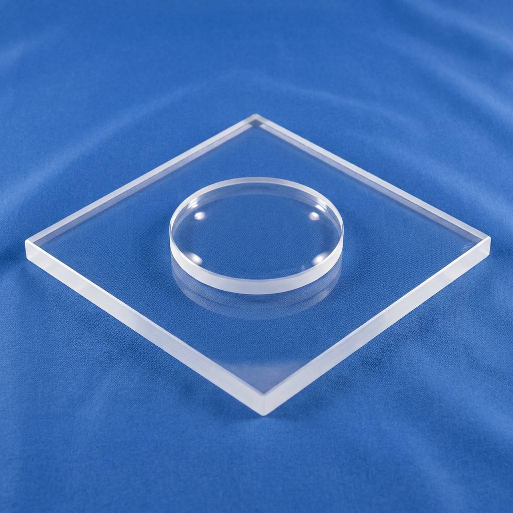
Quartz Glass Plate for Optical Window Fused Silica High Transmittance
- UV Transmittance: > 92% @ 254 nm
- Surface Polish: 20/10 Scratch-Dig
- Roughness (Ra): ≤ 0.5 nm Superpolish

Quartz Viewport Glass Plate Vacuum Chamber Fused Silica Custom Size
- Leak Rate: < 1×10⁻¹⁰ mbar·l/s
- Pressure Rating: UHV to 1.5 MPa
- Mount Type: CF/KF Flange Sealing
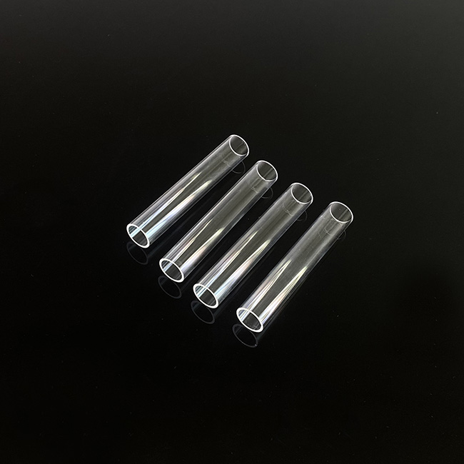
Large Diameter Clear Quartz Borosilicate Glass Tube round Fused Silica
- OD Capability: Ø 100 mm – 520 mm
- Wall Uniformity: Sdeviation ≤ 0.15 mm
- Forming Tech: Continuous Horizontal Draw
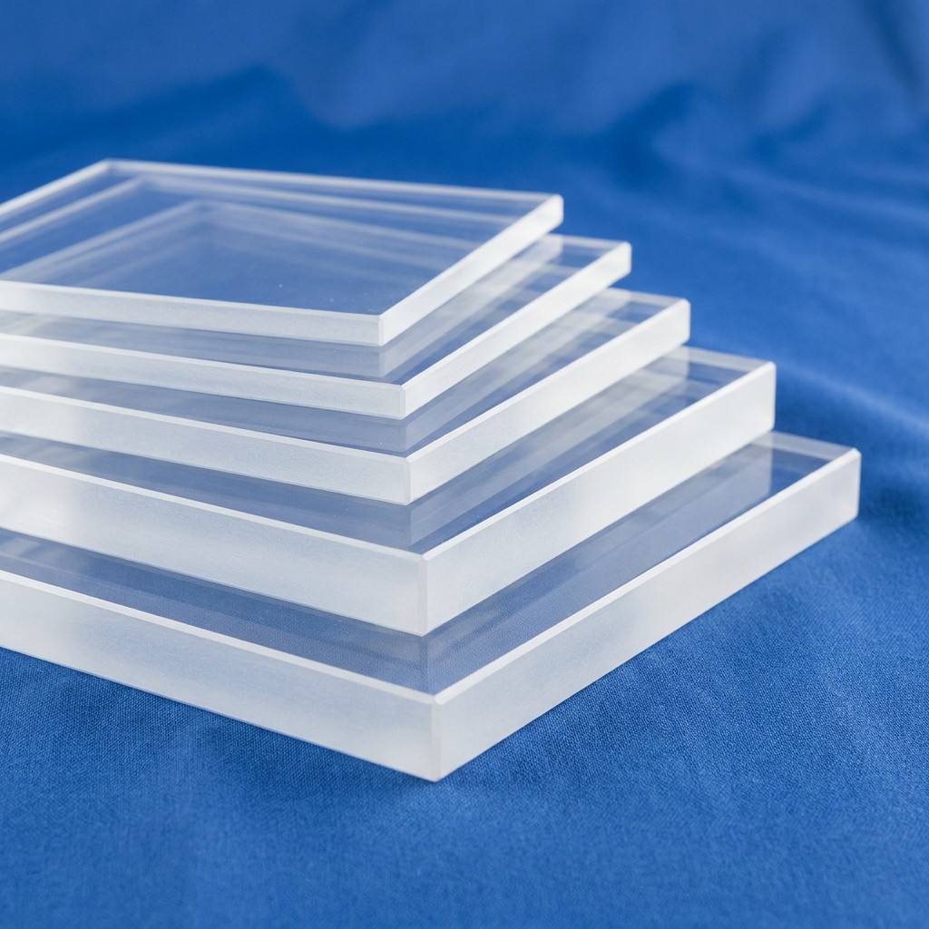
Quartz Fireplace Viewing Glass Plate Heat Resistant Fused Silica
- Continuous Temp: 1100 °C Working Limit
- Thermal Expansion: 5.5 × 10⁻⁷ /°C
- Edge Finishing: C-Profile Beveled Seam
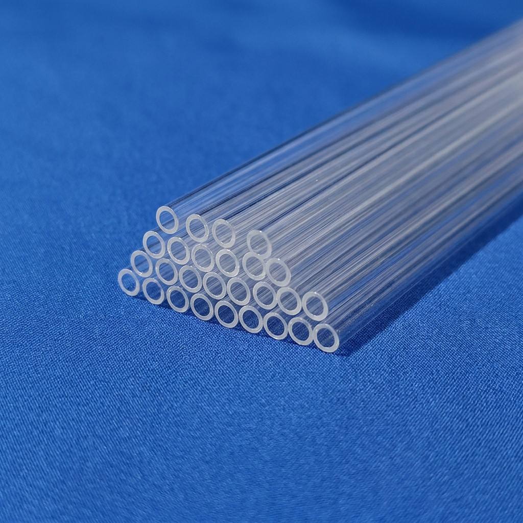
Quartz Glass Tube Raw Stock Clear Fused Silica Transparent Pipe Blank
- Standard Stock: OD 2 mm to 300 mm
- Purity: 99.99% SiO&sub2; Minimum
- End Condition: Cut, Fire-Polished, Flanged

Quartz Substrate Plate for Semiconductor Fused Silica Clear Polished
- TTV (Total Thickness): < 2 μm across 200mm
- Surface Quality: 10/5 Scratch-Dig Class
- Metal Contaminants: ≤ 10 ppb Fe, Cu, Ni
Rooted in China's Quartz Capital: VEZLO Quartz Products
Strategically situated in Tuofeng Township, Donghai County (Lianyungang, Jiangsu Province)—globally recognized as China's Quartz Capital—VEZLO Quartz Products Co., Ltd. controls a modern 50-mu (≈33,000 m²) production complex backed by substantial fixed capital assets and an unbroken industrial upstream-to-downstream supply chain.
Our engineering division executed the prestigious Jiangsu Provincial Science & Technology Support Project, successfully developing the 320 mm high-purity quartz tube for VLSI semiconductor circuits. Expanding this frontier, our newly developed 520 mm ultra-large-diameter high-purity quartz tube has advanced through national new product reviews, providing China-direct capability for 300 mm (12-inch) and 450 mm (14-inch+) wafer diffusion and dry oxidation reactors.

Procurement Trajectories & Technological Evolution (2025–2030)
The optical quartz landscape is shifting rapidly under the dual pressures of advanced semiconductor node scaling (≤ 3 nm) and high-power kW-class industrial laser adoption. Procurement managers must adapt to structural changes in material specifications, geopolitical supply chains, and fabrication tolerances.
Transition to Large-Bore 520 mm Furnace Tubes
As semiconductor fabrication migrates toward advanced vertical stacking (3D NAND beyond 300 layers and GAAFET nodes), wafer processing tubes face extreme dimensional demands. Sourcing trends highlight an accelerated switch from multi-piece quartz assemblies to seamless large-diameter continuously drawn tubes (OD 450 mm to 520 mm) that minimize stress failure risks and particle shed inside LPCVD and ALD tooling.
Sub-Nanometer Roughness for Ultra-High LIDT Optics
With industrial fiber lasers surging past 20 kW and ultrafast picosecond/femtosecond systems scaling rapidly, traditional polish specifications (Ra ∼ 1 nm) are no longer sufficient. High-damage-threshold applications require super-polished synthetic fused silica (Ra ≤ 0.2 nm) with low bulk hydroxyl (OH < 1 ppm) content to eliminate thermal lensing, photo-darkening, and catastrophic laser breakdown.
Direct-from-Origin Integrated Sourcing
Western procurement departments are actively reducing tiered broker markups by partnering directly with integrated producers in Donghai, China. Sourcing raw high-purity quartz sand, continuous ingot melting, precision CNC milling, and optical metrology under a single facility roof lowers lead times from 16 weeks to under 25 business days while mitigating shipping damage vectors.
Comprehensive Material Property Specification Matrix
Quantitative comparative data for engineering design teams specifying transparent fused quartz, synthetic fused silica (JGS1), and optical crown borosilicate.
| Physical Parameter | Standard Fused Quartz (JGS2) | Synthetic Fused Silica (JGS1) | Borosilicate Glass (3.3) | Engineering Significance |
|---|---|---|---|---|
| Chemical Composition | SiO&sub2; ≥ 99.99% | SiO&sub2; ≥ 99.9999% | 81% SiO&sub2;, 13% B&sub2;O&sub3; | Determines impurity leaching in wet chemistry |
| Spectral Range (T > 80%) | 260 nm – 2500 nm | 185 nm – 2500 nm | 350 nm – 2000 nm | Critical for UV curing, lithography, & laser windows |
| Density (@ 20°C) | 2.20 g/cm³ | 2.201 g/cm³ | 2.23 g/cm³ | Payload calculation in aerospace observation viewports |
| Refractive Index (nd @ 587.6nm) | 1.4585 | 1.4584 | 1.4730 | Focal shift and dispersion modeling in optical lenses |
| Coeff. of Thermal Expansion (CTE) | 5.5 × 10⁻⁷ /°C | 5.2 × 10⁻⁷ /°C | 32.5 × 10⁻⁷ /°C | Thermal shock safety; quartz is 6x more stable than boro |
| Softening Point | 1683 °C | 1730 °C | 820 °C | Determines high-temperature furnace operating envelope |
| Annealing Point | 1215 °C | 1180 °C | 560 °C | Stress relief threshold after torch glassblowing |
| Dielectric Constant (ε @ 1MHz) | 3.75 | 3.80 | 4.60 | Ultra-low RF loss in semiconductor microwave antennas |
| Surface Roughness Limit (Ra) | ≤ 0.5 nm | ≤ 0.2 nm (Atomic Grade) | ≤ 1.5 nm | Minimizes high-power laser beam scatter |
Frequently Asked Technical & Procurement Questions
Clear, unequivocal answers addressing tolerance boundaries, material grades, logistics, and quality assurance protocols for high-precision optical quartz components.
How do I choose between Fused Quartz (Natural) and Fused Silica (Synthetic)?
Synthetic Fused Silica is synthesized chemically from volatile silicon precursors (such as SiCl&sub4;) via vapor flame hydrolysis. It is structurally pure (SiO&sub2; ≥ 99.9999%), virtually free from metallic elements (total impurities < 0.1 ppm), and exhibits no UV absorption down to 185 nm. Specify synthetic fused silica for DUV excimer laser optics, semiconductor reticle photomasks, and precision laser window substrates prone to photo-darkening.
What are the achievable manufacturing tolerances for CNC machined quartz parts?
- Outer Dimensions & Diameters: ± 0.02 mm (standard) down to ± 0.005 mm on demand.
- Center Thickness & Step Grooves: ± 0.01 mm.
- Hole Pitch & True Position: ± 0.015 mm.
- Optical Surface Polish: Military standard MIL-PRF-13830B 20/10 or 10/5 Scratch-Dig.
- Transmitted Wavefront Error: λ/4 to λ/10 per 25 mm diameter at 632.8 nm.
- Parallelism: ≤ 5 to 10 arcseconds.
Why is hydroxyl (OH−) content critical when sourcing optical quartz?
What makes VEZLO Quartz's large-diameter 520 mm tubes unique in China?
How do you prevent shipping breakage and surface scratching during export?
Can I order custom prototypes before committing to mass production volume?
Engineering RFQ Protocol: The 6 Key Parameters
To expedite technical reviews and ensure pricing accuracy, engineering buyers are encouraged to formulate inquiries using our standardized six-point engineering specification framework.
Spectral Grade & Optical Transmission
State the operating wavelength (e.g., 193 nm DUV, 355 nm UV, 632.8 nm HeNe, 1064 nm Nd:YAG, or broadband 2000+ nm). Specify whether JGS1 (Synthetic Fused Silica), JGS2 (Optical Fused Quartz), or JGS3 (Infrared Fused Silica) is required to ensure optimal laser transmission and prevent photo-darkening.
Geometrical Dimensions & Tolerancing
Provide comprehensive outer diameter (OD), inner diameter (ID), thickness, and length values along with acceptable bilateral tolerances. Include step groove geometries, beveling angles (e.g., 0.5 mm × 45°), and drilled hole patterns with true position specifications.
Surface Figure & Cosmetic Quality
Specify surface scratch-dig limits according to MIL-PRF-13830B (e.g., 60/40 commercial, 20/10 precision laser grade, or 10/5 ultra-high-power optics). Define transmitted wavefront error (λ/2, λ/4, or λ/10) and parallelism boundaries (< 3 arcmin vs < 10 arcsec).
Thermal & Environmental Pressures
Clarify the thermal operating profile: continuous temperature exposure, ramp-up speeds (°C/min), cycle frequency, and atmospheric context (ultra-high vacuum 10−9 torr, positive pressure MPa, corrosive halogen chemistry, or high-density inductively coupled plasma).
Connect Directly with Our Optical Engineering Division
Whether you are engineering a custom vacuum chamber viewport, integrating multi-hole CNC quartz diffusers, or scaling 520 mm semiconductor diffusion furnace tubes, VEZLO Quartz provides factory-direct precision from China's quartz capital.