Recommended Precision Fused Silica & Quartz Products
Engineered to drawing from raw high-purity natural silica sand (metals ≤20 ppm) to finished semiconductor, optical, and high-temperature quartz parts.
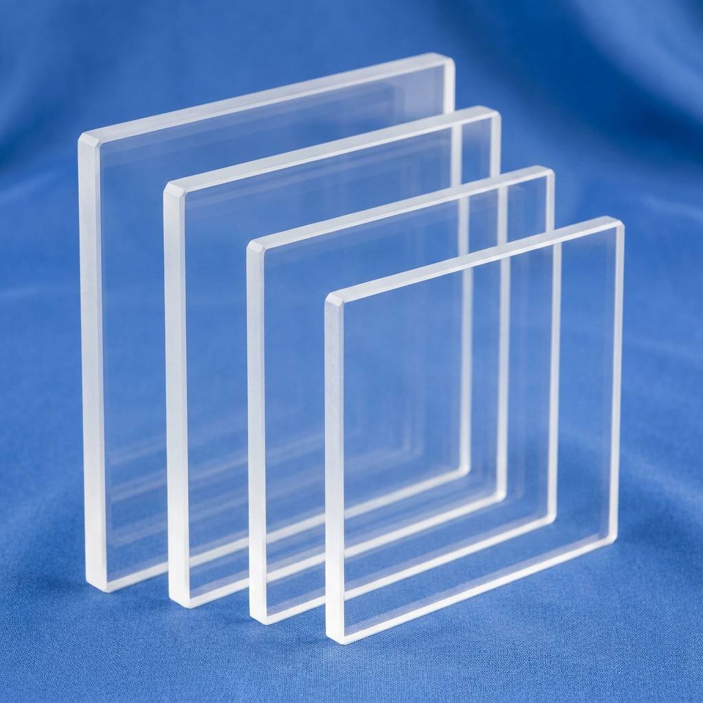
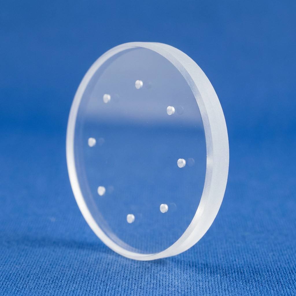

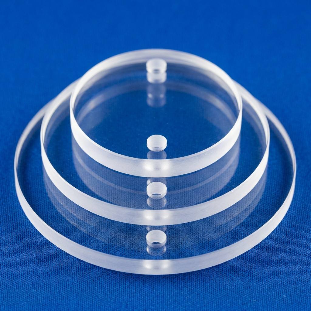


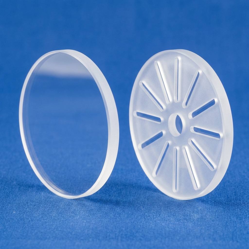
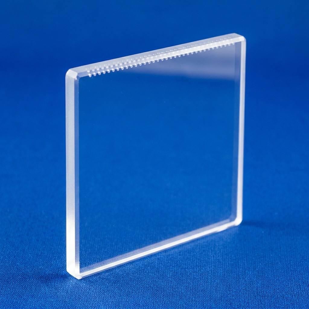
Engineering Overview: Fused Silica & Fused Quartz Metallurgy
In high-reliability industrial manufacturing, selecting between natural fused quartz and synthetic fused silica tubes dictates thermal performance, service lifetime, and operational contamination risks. While the market frequently uses "fused silica" and "fused quartz" interchangeably, senior procurement engineers distinguish them by their precursor chemistry and microscopic morphology.
Natural Fused Quartz is synthesized via electric-arc fusion or oxy-hydrogen gas smelting of high-purity natural silica crystalline quartz sand. The structural integrity of natural quartz offers exceptional creep resistance at extreme temperatures (>1,150°C) and mechanical stiffness, making it the bedrock material for horizontal and vertical wafer processing tubes, thermocouple protection sheaths, and industrial UV curing envelopes.
Synthetic Fused Silica is derived through the gas-phase chemical vapor deposition (CVD) or flame hydrolysis of silicon tetrachloride (SiCl4) or organosilicon precursors. This process eliminates almost all trace metal contaminants (Fe, Al, Ti, Na, K, Li < 0.1 ppm), achieving virtually 100% stoichiometric amorphous silicon dioxide (SiO2). Synthetic silica provides unparalleled UV transmission down to 185 nm and 193 nm (ArF excimer laser lithography) and displays virtually zero bubble incorporation (Class 0 per DIN ISO 10110).
Material Performance Specification Reference Matrix
| Thermal & Physical Property | Semiconductor Grade Fused Quartz | Synthetic Fused Silica (JGS1) | Procurement Significance |
|---|---|---|---|
| SiO2 Purity Level | ≥ 99.995% (≤20 ppm metals) | ≥ 99.9999% (≤0.5 ppm metals) | Prevents wafer gate-oxide contamination |
| Coefficient of Thermal Expansion (CTE) | 5.5 × 10⁻⁷ / °C (20°C–320°C) | 5.2 × 10⁻⁷ / °C | Immunity to rapid thermal shock & quenching |
| Maximum Continuous Service Temp. | 1,150 °C | 1,050 °C (Lower due to OH content) | Crucial for LPCVD and oxidation furnace cycles |
| Softening Point | ≈ 1,683 °C | ≈ 1,600 °C – 1,650 °C | Determines high-temp dimensional sag resistance |
| Deep UV Cutoff Wavelength | 220 nm – 260 nm | 160 nm – 185 nm | Critical for germicidal UV-C and excimer systems |
| Hydroxyl (OH−) Concentration | < 5 ppm – 30 ppm | 150 ppm – 1,200 ppm | Regulates near-IR absorption bands (2.73 μm) |
Integrated Donghai Production Infrastructure
Operating a massive 50-mu (≈33,000 m²) specialized manufacturing campus in Donghai County, Jiangsu Province—internationally acknowledged as the premier quartz production capital of China—our facilities capitalize on fully integrated vertical supply chains. By commanding both raw silica refining and multi-axis finishing, we resolve supply chain volatility while sustaining strict lot-to-lot traceability.
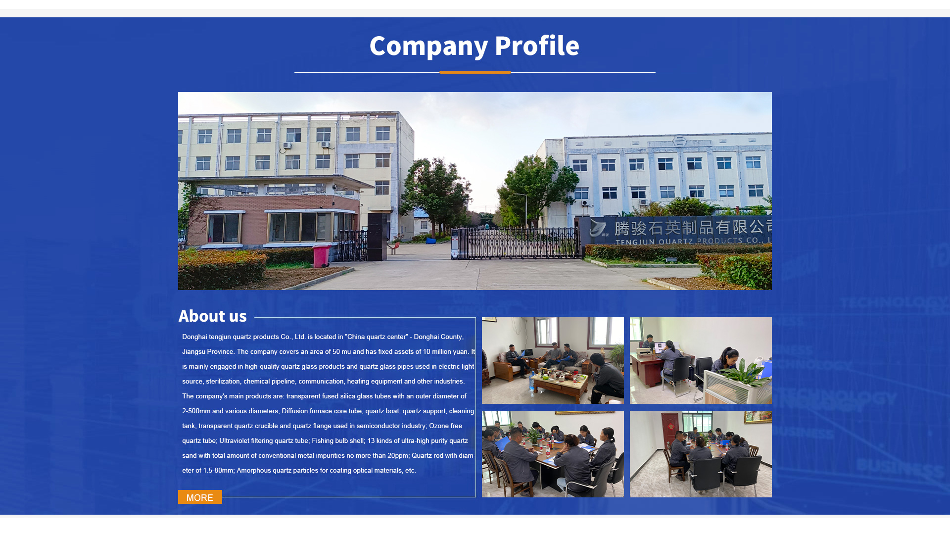
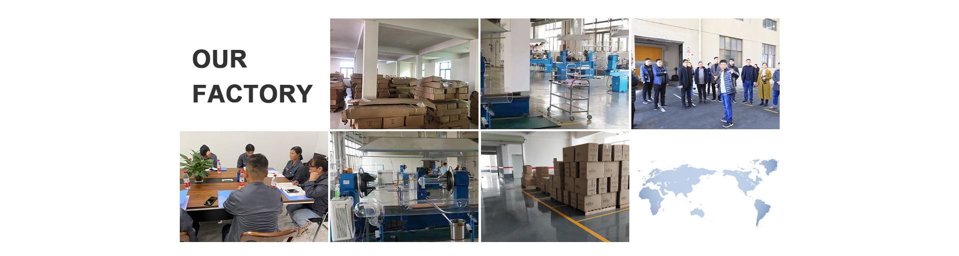

Our 320 mm high-purity quartz tube development was completed under the prestigious Jiangsu Provincial Science & Technology Support (Industrial) Project, reinforcing our status as a state-sanctioned core technology developer. Furthermore, our proprietary 520 mm large-diameter high-purity fused silica furnace tube has passed the initial review for National New Products, solving 12-inch and 14-inch wafer thermal processing bottlenecks for global semiconductor tool builders.
Future Procurement Trends in Fused Silica Tubing
Emerging manufacturing architectures, energy transition imperatives, and chip fabrication milestones are fundamentally restructuring how supply chain executives procure quartzware.
1. Diameter Scaling (520 mm+) for Next-Gen Wafers
As semiconductor fabs scale towards sub-2nm nodes and 3D NAND layering (beyond 300 layers), oxidation and diffusion furnaces require tubes exceeding 500 mm in diameter. Tool OEMs demand extreme wall thickness uniformity (±0.2 mm) and zero camber across 2.5-meter furnace tube lengths to protect robotic wafer handling end-effectors.
2. Trace Alkali Metal Suppression (≤0.05 ppm)
Advanced transistor gate geometries (GAAFET) cannot tolerate mobile ion contamination. High-temperature furnace tubes are shifting toward synthetic inner liner barriers or chemical gas-phase de-hydroxylation treatments to eliminate Na, K, and Li diffusion under long thermal exposure profiles.
3. Transition to Monolithic Cold CNC Machining
Traditional manual flame-welding introduces micro-stresses, localized cristobalite crystallization, and geometric tolerances beyond ±0.5 mm. Modern enterprise buyers are specifying 5-axis ultrasonic CNC machined and monolithic ground quartz assemblies to guarantee ±0.05 mm dimensional repeatability.
Technological Development Trends in Silica Glass Fabrication
From plasma-assisted chemical polishing to dopant engineering, new manufacturing methodologies are elevating fused silica from passive vessels into high-performance active reactor components.
Ozone-Free Doped Silica
Selective titanium/cerium doping precisely blocks the 185 nm VUV line while maintaining 90%+ transmission at 254 nm germicidal wavelength, mitigating hazardous ozone build-up in closed-circuit fluid sterilization.
Plasma Fire Polishing
Atmospheric inductively-coupled plasma polishing eliminates micro-fractures left by diamond grinding, boosting mechanical bursting pressure in high-pressure reactor tubes by over 40%.
Hydroxyl Content Engineering
Low-OH synthesis (<1 ppm) suppresses infrared water absorption bands at 2.2 μm and 2.73 μm, preventing thermal efficiency loss in high-output industrial filament radiators and halogen heat chambers.
Direct 3D Glass Sintering
Pioneering additive fused silica suspension sintering enables internal microfluidic channels, complex internal cooling jackets, and bespoke furnace thermocouple wells without assembly welding joints.
Why Global Tier-1 Buyers Partner with VEZLO Quartz
Managing the procurement of fragile, mission-critical fused quartz components requires technical certainty and operational transparency. Founded upon RMB 10 million in capital assets with an annual R&D commitment exceeding RMB 5 million, our manufacturing operation sets global benchmarks across four core disciplines:
Vertically Integrated Sand-to-Tube Control
By refining 13 distinct grades of ultra-high-purity quartz sand (total metals ≤20 ppm) directly within our Donghai synthesis facilities, we mitigate raw material price shocks and guarantee chemical traceability down to the raw batch lot.
State-Sanctioned R&D Capabilities
Our direct involvement in provincial high-tech initiatives (Jiangsu Provincial S&T Support Project for 320 mm tubes) and National New Product designations ensures clients access tier-1 technical consultation and proprietary drawing feasibility evaluations.
Certified Global Packaging & Rapid SLA
With an audited average inquiry response under 2 hours, multilingual engineering desks, and specialized multi-layer suspension foam crating inside ISPM-15 export-compliant wooden cases, we maintain a zero-breakage export track record across 40+ countries.
Frequently Asked Questions for Quartz Tube Sourcing
Essential technical, financial, and logistical criteria addressed by our senior production engineering team.
What are the maximum dimensional boundaries for clear fused quartz tubes produced in your factory?
How do you prevent devitrification (crystallization) during high-temperature thermal cycling?
What is the exact distinction between standard, ozone-free, and high-purity semiconductor tubes?
Can VEZLO Quartz manufacture bespoke configurations directly from client CAD or STEP files?
What geometric tolerances can your factory sustain on large-diameter quartz tubes?
What testing protocols and quality certifications accompany export deliveries?
How does VEZLO Quartz guarantee zero transit breakage for fragile quartzware exported globally?
Ready to Source High-Purity Fused Silica Direct from the Factory?
Submit your component drawings, sizing parameters, or technical project specifications. Our Donghai materials engineering team provides rigorous DFM analysis, pricing schedules, and lead-time projections within 2 business hours.
Get a Quote