Featured CE Certified Quartz Products for Daejeon High-Tech Fabs
Factory-direct fused silica sheets, custom laser-profiled substrates, CVD/ALD furnace core tubes, and optical viewports machined to micron-level tolerances.

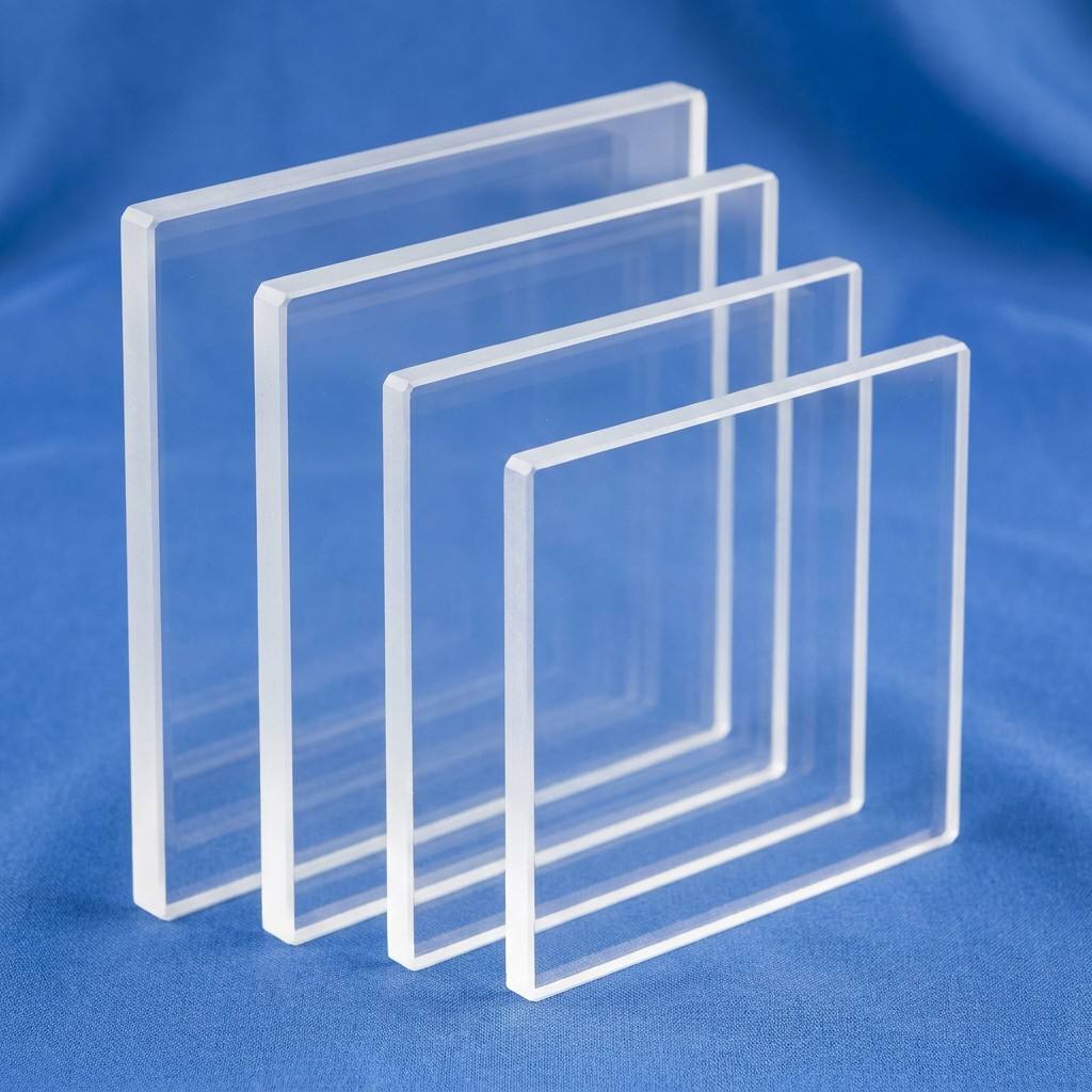
Laser Cut Quartz Glass Plate Fused Silica Precision Custom Size
View Specifications

Quartz Plate 100x100mm 200x200mm Fused Silica Clear Custom Cut
View Specifications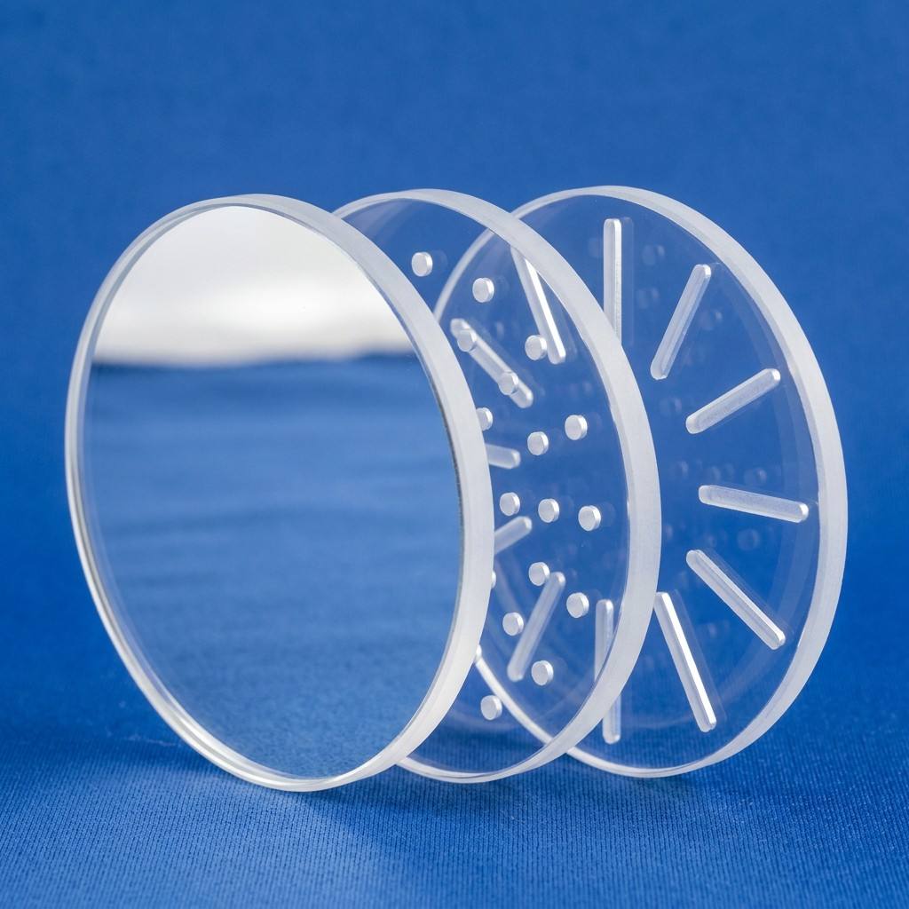
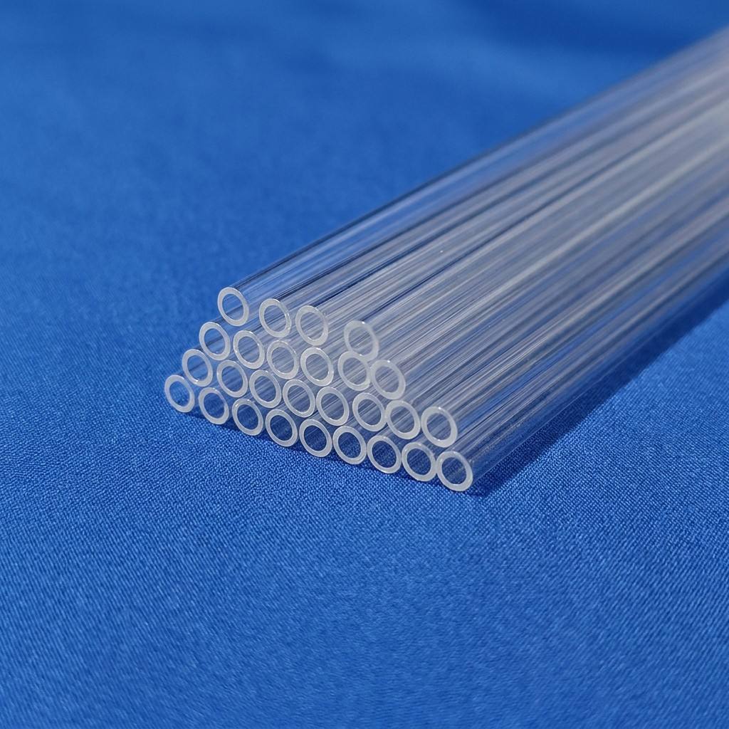
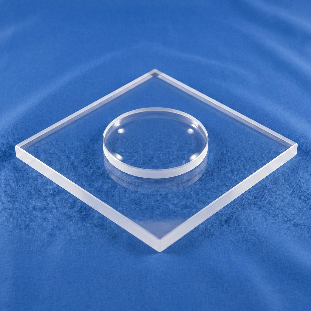
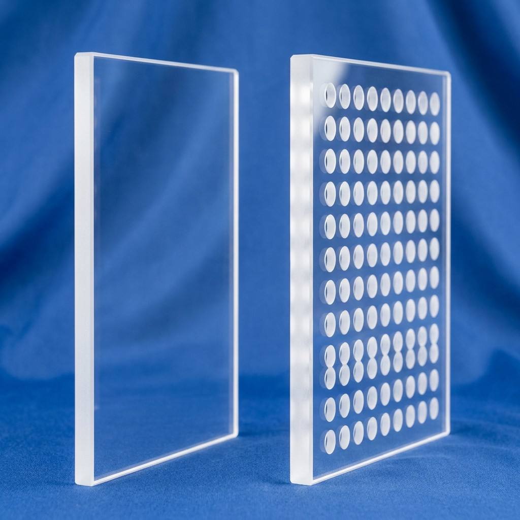
Quartz Glass Plate for Vacuum Chamber Viewport High Purity Custom
View SpecificationsThe Critical Role of CE-Certified Quartz Supports in Advanced Semiconductor & Nanotechnology Metrology
In high-temperature semiconductor processing, materials science research, and atomic layer deposition (ALD), the thermal and mechanical integrity of the substrate support matrix directly dictates yield, baseline repeatability, and process chamber cleanliness. Daejeon—as the scientific nucleus of South Korea centered around Daedeok Innopolis, the Korea Advanced Institute of Science and Technology (KAIST), and the Electronics and Telecommunications Research Institute (ETRI)—demands quartzware with uncompromising physical specifications. Quartz supports, wafer boats, pedestal rings, and furnace process tubes serve as the physical barrier and carrier during extreme thermal regimes, often operating continuously between 900°C and 1250°C.
Fused quartz and synthetic fused silica exhibit unique material characteristics that make them irreplaceable compared to alumina, silicon carbide, or technical ceramics. Foremost is an exceptionally low coefficient of thermal expansion (α ≈ 5.5 × 10⁻⁷ /°C), granting virtual immunity to catastrophic thermal shock. A quartz support assembly can be repeatedly cycled from high-temperature diffusion zones into room ambient atmosphere without micro-fracturing or dimensional creep. However, ensuring that these components function stably inside sub-micron semiconductor fabrications requires stringent control over material provenance, trace alkali metal contamination, and microscopic structural homogeneity.
Material Purity, Devitrification Kinetics, and Hydroxyl (OH) Content Optimization
The operational lifespan of quartz supports in CVD, LPCVD, and diffusion equipment is predominantly bounded by devitrification—the phase transformation of amorphous silica into crystalline cristobalite. Cristobalite undergoes an abrupt α-to-β volumetric transition at 220°C, introducing severe local shear stresses that induce structural micro-cracking, flaking, and fatal wafer contamination. This devitrification process is catalyzed primarily by surface alkali impurities (notably Sodium [Na], Potassium [K], and Lithium [Li]) and heavy transition metals (Iron [Fe], Copper [Cu]).
Our manufacturing methodology ensures total metallic impurities are strictly constrained below ≤ 20 ppm across conventional grades, with specialized semiconductor lots refined to sub-10 ppm thresholds. Furthermore, by precision-tuning the hydroxyl [OH-] radical concentration during multi-stage oxy-hydrogen flame fusing and electrical vacuum furnace melting, we regulate the glass annealing point (≈ 1215°C) and strain point (≈ 1120°C). Low-OH quartz resists structural sagging under gravitational load at prolonged 1150°C+ holding times, providing Daejeon's pilot lines with geometrically unyielding wafer pitch tolerances (±0.05 mm) across multiple manufacturing batches.
| Property Parameter | High-Purity Fused Quartz (Natural) | Synthetic Fused Silica (Chemical Precursor) | Operational Significance for Daejeon Facilities |
|---|---|---|---|
| SiO2 Purity | ≥ 99.99% (≤ 20 ppm metals) | ≥ 99.9999% (≤ 1 ppm metals) | Prevents metal ion diffusion into silicon active layers during thermal drive-in. |
| Coefficient of Thermal Expansion | 5.5 × 10⁻⁷ / °C | 5.2 × 10⁻⁷ / °C | Enables rapid thermal insertion/pulling cycles without wafer-support warpage. |
| Softening Point / Strain Point | 1683°C / 1120°C | 1600°C / 1070°C | Natural quartz provides higher creep resistance in horizontal/vertical furnace tubes. |
| Deep UV Transmittance (248/193 nm) | 60% – 85% (Grade dependent) | > 90% (Optical excimer grade) | Synthetic silica chosen for laser beam path windows; natural for thermal supports. |
| Dielectric Constant (1 MHz) | 3.75 | 3.80 | Optimal for high-frequency RF-powered PECVD and dry etching support pedestals. |
Serving the R&D Clusters and Industrial Giants of Daejeon
Strategically supporting Daedeok Innopolis, corporate incubation centers, and university research facilities with rapid-delivery, CE-certified high-temperature components.
Semiconductor Wafer Processing & Pilot Fabs
From KAIST's cleanrooms to advanced fab facilities in the greater Chungcheong corridor, our quartz supports, cantilever beams, and vertical wafer boats maintain strict slot parallelism. Engineered to withstand harsh hydrofluoric (HF) acid cleaning cycles and aggressive plasma etch environments without micro-fissuring.
Solar Photovoltaic & Clean Energy Synthesis
Daejeon serves as South Korea's think tank for next-generation perovskite and tandem heterojunction solar cell development. Our ultra-large diameter quartz process tubes (up to 520 mm) and high-purity quartz crucibles provide non-contaminating thermal zones for silicon ingot crystallization and dopant diffusion.
Quantum Physics, Nanotech & Optical Metrology
Daedeok's photonic and quantum researchers require vacuum viewports and laser-cut fused silica window plates featuring minimal wavefront distortion (λ/4 or better) and low birefringence. Our double-side optical polishing provides ultra-clear optical access inside cryogenic and ultra-high-vacuum (UHV) experimental chambers.
Technological Evolution and Procurement Trends in Daejeon (2025–2030)
How South Korea's national strategic semiconductor roadmap is reshaping supply chain specifications for fused quartz components.
South Korea’s mega-semiconductor cluster initiatives extending from Gyeonggi down into the Daejeon/Chungcheong corridor are accelerating the demand for localized engineering collaboration and faster component qualification cycles. In Daejeon's R&D ecosystem, several pronounced trends are defining technical purchasing behavior:
1. Scaling to Larger Substrate Geometries
As research shifts from traditional 150 mm/200 mm wafers toward high-throughput 300 mm platforms and 3D NAND vertical structures, quartz hardware must withstand greater mechanical moment forces. Support fingers and cantilever rods require tighter geometric stiffness and fire-polished stress-relieved junctions to prevent gravitational deflection at 1200°C.
2. Rigorous EU & CE Export Directives
Daejeon-based semiconductor equipment builders (OEMs) export automated wet benches, thermal processing tools, and deposition reactors worldwide. Equipment destined for European fabs mandates full CE certification under the Machinery Directive (2006/42/EC) and Pressure Equipment Directive (PED). Sourcing CE-certified quartz components simplifies total system homologation.
3. Direct Sourcing for Lead-Time Compression
Procurement teams are actively bypassing multi-tier broker networks in favor of direct manufacturer relationships with primary quartz hubs like Donghai. Direct access to raw high-purity sand processing, continuous melting, and dedicated glassblowing workshops reduces prototype delivery lead times from months down to 2–3 weeks.
Direct Manufacturer Infrastructure Rooted in China's Quartz Capital
Combining raw mineral refinement, advanced flame-working craftsmanship, and rigorous export quality assurance under a single verified umbrella.
Donghai 50-Mu Base
Operating a 33,000 m² production complex backed by RMB 10 million in fixed assets, directly accessing world-class natural crystal resources and refined quartz sand processing.
Government R&D Recognition
Developers of the 320 mm high-purity tube recognized under the Jiangsu Science & Technology Support Project, and newly pioneered 520 mm large-diameter furnace core tubes.
Dual Cold & Hot Processing
Equipped with 5-axis CNC ultrasonic milling, high-precision laser profiling, and master flame-working lathes capable of complex manifold and wafer boat synthesis.
Verified Export Standards
Onsite-verified enterprise with average technical response times under 2 hours, rigorous cleanroom double-vacuum packaging, and 50% repeat client orders worldwide.
Frequently Asked Questions for Daejeon Procurement Engineers
Clear answers addressing customs, dimensional tolerances, material certifications, and shipping logistics into South Korea.
Why is CE Certification necessary for quartz supports supplied into Daejeon?
What dimensional tolerances can be guaranteed on custom laser-cut and ground quartz plates?
How fast can custom prototypes and batch orders be delivered to Yuseong-gu / Daedeok Innopolis?
How do you mitigate particle contamination and transit breakage for fragile quartzware?
Can VEZLO reproduce obsolete or custom quartz boats and supports from physical samples?
What documentation and quality certifications accompany each delivery to South Korea?
Accelerate Your Quartz Sourcing for Daejeon Facilities
Connect directly with VEZLO Quartz's technical engineering team. Send your CAD drawings (.DWG, .DXF, .STEP, or PDF) for immediate feasibility reviews, rapid manufacturing schedules, and direct factory pricing within 2 hours.