
Quartz Photomask Substrate Plate Fused Silica UV Grade Ultra Thin
Deep UV transmittance (>90% at 193–248nm), surface roughness Ra < 0.5nm, minimal bubble class 0.
Engineered to comply with rigorous JIS B7071 and SEMI standards, our export-ready fused silica substrates, grooved carriers, and viewports provide seamless compatibility for Osaka's optoelectronic and semiconductor toolmakers.
Deep UV transmittance (>90% at 193–248nm), surface roughness Ra < 0.5nm, minimal bubble class 0.
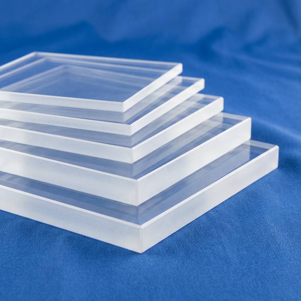
Continuous 1100°C thermal endurance, thermal shock resistance ΔT > 1000°C, zero thermal expansion stress.

CNC micro-machined pitch tolerance ±0.02mm, flame-polished groove edges to eliminate wafer micro-chipping.
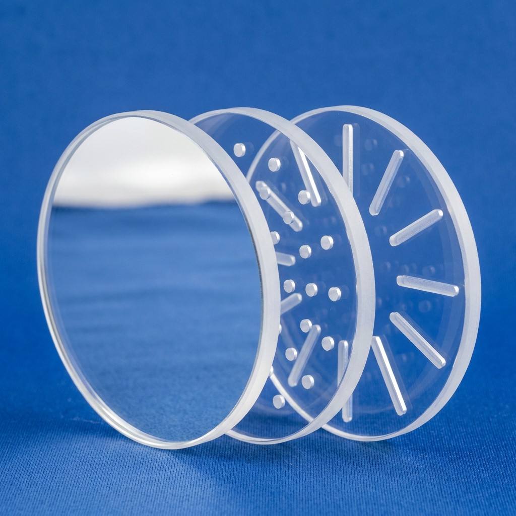
Optical clarity, high dielectric strength, custom chamfered margins for UV curing arrays and display stages.
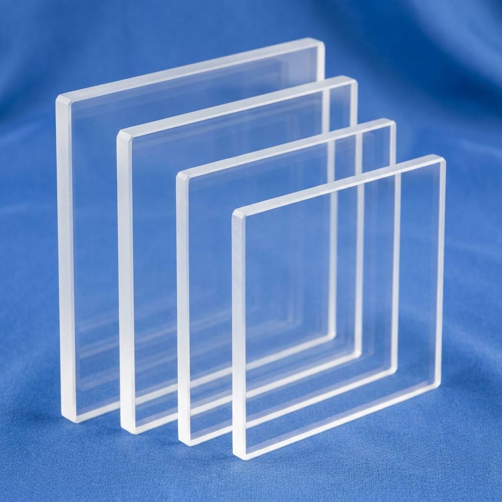
CO₂/Picosecond laser precision profiled, zero micro-crack kerf, complex internal geometry execution.

C-cut beveling, precision lapped parallelism < 15 arcseconds, superior mechanical edge resistance.

High-vacuum seal tolerance, CF/ISO flange match, pressure-tested viewing port for plasma etch and CVD.
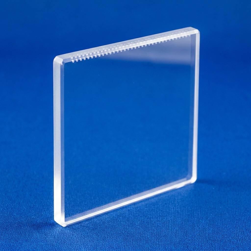
Laser interferometer verified λ/10 or λ/20 surface accuracy, scratch-dig 20/10, dual-side optical grade polishing.
The manufacturing ecosystem in the Kansai region—spanning Osaka, Kyoto, and Hyogo—represents one of the world's dense clusters of precision optical instrumentation, advanced chemical synthesis, flat panel display (FPD) manufacturing, and green power electronics. For decades, industrial procurement officers in Osaka's prominent districts such as Higashiosaka, Yodogawa, and Sakai have faced an ongoing dual challenge: maintaining the zero-defect material standards required by domestic Japanese manufacturing while controlling baseline bill-of-materials (BOM) costs in an inflationary global market.
As a vertically integrated leader headquartered in Donghai County, Jiangsu—widely recognized as China's Quartz Center—our manufacturing facilities bridge this precise gap. By owning the processing chain from high-purity quartz sand refined down to ≤20 ppm total metallic impurities to fully synthesized fused silica ingots, precision cold CNC machining, and cleanroom fire-polishing, we eliminate middle-tier trading markups while offering certified dimensional and chemical compliance.
Procurement teams across Osaka often evaluate whether electric-fused quartz or synthetic fused silica serves their specific operational budget and physical criteria:
| Physical / Chemical Parameter | High-Purity Fused Quartz (Donghai) | Synthetic Fused Silica (Optical) | Procurement Relevance for Osaka Fabs |
|---|---|---|---|
| SiO₂ Purity Level | ≥ 99.99% | ≥ 99.9999% | Prevents heavy metal ionic migration in wafer chambers |
| Thermal Expansion Coeff. (0–300°C) | 5.5 × 10⁻⁷ / °C | 5.2 × 10⁻⁷ / °C | Near-zero thermal shock expansion during rapid thermal processing (RTP) |
| Continuous Service Temperature | 1,100 °C | 1,050 °C | Critical for LPCVD and oxidation furnace long runs |
| Hydroxyl (OH⁻) Concentration | < 5 ppm to 30 ppm (Dry grade) | 100 to 1,200 ppm (Grade dependent) | High OH absorbs mid-IR; low OH protects transmission stability |
| Transmittance Range | 260 nm – 2,500 nm | 185 nm – 2,500 nm | Specifies usability in Deep-UV photolithography vs. general UV curing |
From cleanroom fabrication suites in Osaka Bay to high-tech research clusters in Senri Life Science Center and Kyoto University research corridors, our fused silica components integrate into mission-critical processes.
In the Yodogawa and Higashiosaka precision fab clusters, our grooved fused silica plates and high-diameter diffusion tubes (OD up to 520 mm) serve as low-particulate wafer boats, batch holders, and chamber process viewports for 200 mm and 300 mm wafer processing lines.
Precision lithography equipment manufacturers require optical flats and ultra-thin photomask plates featuring low birefringence and flawless UV throughput. Our dual-side polished quartz plates prevent chromatic aberration across high-power UV exposure machinery.
Within the Osaka Bay energy corridor, battery cell developers leverage our thermal-shock resistant quartz crucibles, sight glasses, and reaction tubes for lithium-ion battery precursor calcination and high-temperature cathode material sintering without cross-contamination.
Procurement within Japan’s manufacturing heartland has transitioned from standard transactional replenishment to strategically resilient supply chain integration. Analysis of incoming project drawings and inquiries from Japanese engineering firms highlights several noticeable shifts:
1. Demand for Sub-Nanometer Surface Roughness on Photomasks: With next-generation power electronics (SiC and GaN) taking root in Kansai's academic-industrial testbeds, photomask substrate plates demand flatness exceeding λ/10 and surface finishes with Ra values falling below 0.3 nm to eliminate projection scatter.
2. Large-Diameter Quartz Core Envelopes for Oxidation: Transitioning toward domestic semiconductor capacity resilience has revitalized Japanese demand for 300 mm wafer diffusion furnace tubes. Our provincial award-winning 320 mm tubes and newly validated 520 mm large-diameter tubes directly answer this requirement without prolonged domestic lead times.
3. Comprehensive Export Verification & Traceability: Osaka buyers place maximum emphasis on E-E-A-T and supplier reliability. Mill test certificates detailing precise trace metal breakdowns (Fe, Al, Ti, Cu, Cr), accompanied by third-party dimensional CMM coordinate reports, are now prerequisites for baseline vendor onboarding.
Direct from Donghai County's processing heartland, our integrated manufacturing infrastructure ensures consistency, speed, and precision for your most demanding quartz projects.
Operating a 50-mu specialized manufacturing infrastructure with RMB 10 million in fixed assets, delivering end-to-end control from high-purity quartz sand melting to CNC cold-working and laser finishing.
Our 320 mm high-purity quartz tube development was completed under the Jiangsu Provincial Science & Technology Support Project, while our 520 mm large-diameter tube completed national new product technical review.
All precision optical quartz items and thin plates are packed with custom pearl cotton, internal shock absorbing liners, vacuum bags, and certified non-fumigation plywood crates for safe transit to Kansai International Airport (KIX) and the Port of Osaka.
Clear answers covering international logistics, technical tolerances, certification documents, and custom fabrication workflows.
Submit your 2D/3D CAD drawings (DXF, DWG, STEP, PDF) or custom bill of materials. Our technical team reviews mechanical tolerances, optical specifications, and thermal requirements with an average reply time within 2 hours.
Send an Inquiry