Featured Fused Silica Windows & Quartz Components
Directly supplied from Donghai’s integrated synthetic and fused silica manufacturing hubs to Singapore's cleanrooms and engineering lines.
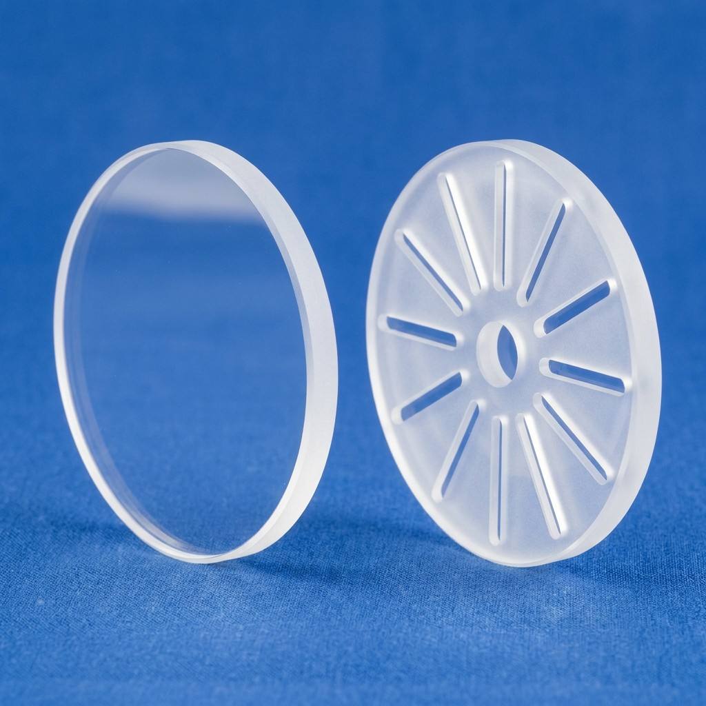
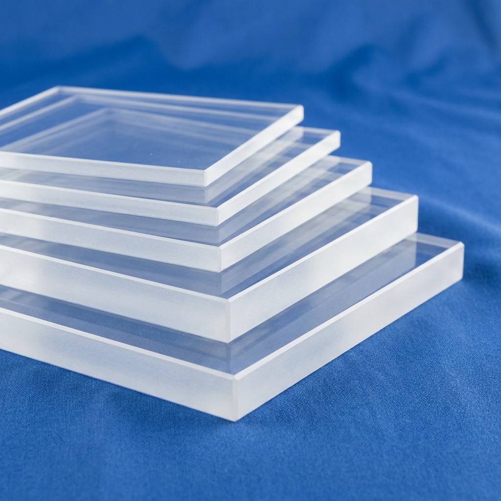


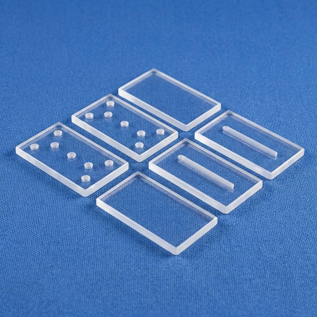

Engineering Fused Silica Windows for High-Precision Applications
Fused silica represents the benchmark material in ultraviolet, visible, and near-infrared optical systems where thermal shock immunity, extreme optical homogeneity, and mechanical integrity cannot be compromised. For optical design engineers and procurement authorities across Singapore’s semiconductor fabrication plants, medical device developers, and national research institutes (A*STAR), distinguishing between synthetic fused silica (chemical vapor synthesis) and natural fused quartz (electric or gas fusion) is critical for system reliability.
VEZLO Quartz manufactures fused silica substrates under tightly calibrated CNC cutting, diamond-wheel surface grinding, and pitch-polishing cycles. Our proprietary annealing schedule alleviates internal mechanical stress, achieving residual birefringence lower than 5 nm/cm. Whether executing sub-millimeter thickness tolerances down to 0.3mm or multi-layer dielectric anti-reflective (AR) coatings, each component is individually characterized utilizing Zygo phase-shifting interferometers and spectrophotometric analysis.
| Physical / Optical Property | JGS1 (Synthetic Silica / UV Grade) | JGS2 (Fused Quartz / Optical Grade) | JGS3 (Infrared Fused Quartz) |
|---|---|---|---|
| Transmission Range | 185 nm – 2,500 nm (Deep UV) | 220 nm – 2,500 nm (Standard Optic) | 260 nm – 3,500 nm (IR Optimized) |
| OH Content (Hydroxyl) | ≥ 1,200 ppm (Water Peak Absorption) | 150 – 200 ppm | ≤ 5 ppm (Water-Free IR Band) |
| Thermal Expansion Coeff. (CTE) | 5.5 × 10⁻⁷ / °C (20°C to 320°C) | 5.5 × 10⁻⁷ / °C | 5.5 × 10⁻⁷ / °C |
| Maximum Working Temp (Continuous) | 1,100 °C | 1,150 °C | 1,150 °C |
| Surface Quality (Scratch-Dig) | 20/10 or 10/5 (Laser Quality) | 40/20 or 60/40 | 40/20 or 60/40 |
| Refractive Index Tolerance | ± 1 × 10⁻⁴ (nd = 1.458) | ± 2 × 10⁻⁴ | ± 2 × 10⁻⁴ |
Mission-Critical Deployment Across Singapore Industry Hubs
Engineered precisely for the unique demands of Singapore’s high-tech industrial nodes, cleanroom standards, and deep-tech innovation corridors.
Wafer Fabs (Woodlands & Tampines)
In high-density semiconductor fabrication clusters across Woodlands, Tampines, and Pasir Ris, fused silica windows are utilized within plasma etch chambers, rapid thermal processing (RTP) equipment, and LPCVD reactors. Their inertness against halogen chemistries (NF₃, CF₄) and high thermal shock resistance ensure uninterrupted process monitoring and zero micro-particle shedding.
Laser & Optics Clusters (Jurong Innovation District)
Advanced manufacturing facilities and laser system integrators situated within the Jurong Innovation District (JID) rely on double-side polished fused silica windows for high-power fiber laser cutting heads, beam splitters, and galvanometer scanning units. With high laser-induced damage thresholds (LIDT > 10 J/cm² at 1064nm, 10ns), our windows protect valuable internal optics without wave-front distortion.
Biomedical Diagnostics (Tuas Biomedical Park)
Tuas Biomedical Park and Biopolis-based research platforms require fused silica plates for flow cytometry flow cells, spectrophotometer optical cells, and fluorescence microscopy windows. The absolute lack of autofluorescence in UV-grade fused silica guarantees ultra-high signal-to-noise ratios during molecular assays and DNA sequencing procedures.
Strategic Trends Reshaping Singapore’s Quartz & Silica Sourcing
Singapore holds an indispensable role as the hub of Southeast Asia’s advanced semiconductor manufacturing and regional photonics distribution. Over the past 36 months, several fundamental shifts have redefined how procurement managers in Singapore source optical glass and silica components:
With Tier-1 global wafer foundries committing multi-billion-dollar capacity upgrades in Singapore, fab operators are moving away from single-source high-cost regional vendors to direct China Tier-1 manufacturing relationships to secure supply continuity and hedge cost inflation.
Rising implementation of deep UV-C (222nm and 254nm) sterilization fixtures across healthcare, aerospace, and mass transit has escalated demand for synthetic silica windows capable of sustained deep-UV transmission without solarization or color-center formation.
Miniaturization of spectroscopic and LiDAR sensors has spiked demand for micro-machined fused silica sheets (0.3mm to 0.8mm) with laser-cut chamfers, CNC-milled stepped edges, and custom apertures conforming to strict optical packaging constraints.
Leveraging direct air cargo connectivity between Shanghai/Lianyungang and Singapore Changi Airport (SIN), engineering prototypes and urgent fab maintenance replacement windows now achieve transit cycles within 3 to 5 business days.
Why Singapore Engineering Teams Partner with VEZLO Quartz
Combining natural raw material dominance in Donghai with comprehensive precision optical machining capabilities.
Integrated Raw Material Base
Operating a dedicated 50-mu (≈33,000 m²) manufacturing complex in Donghai County—China's undisputed Quartz Capital—we secure primary access to ultra-high-purity quartz sand (≤20 ppm impurities across 13 specialized grades). This upstream vertical integration eliminates raw material shortages, prevents internal inclusion variances, and provides direct cost control passed down to wholesale buyers.
R&D Recognition & Tech Leadership
Backed by RMB 10 million in fixed assets and sustained annual R&D expenditures exceeding RMB 5 million, our engineering capabilities were validated by our 320 mm high-purity quartz tube delivery for integrated circuits under the Jiangsu Provincial Science & Technology Support Project. Our 520 mm large-diameter tube recently cleared national new product preliminary reviews.
Rapid Singapore Export Protocol
With verified on-site third-party factory audits and Alibaba Trade Assurance backing, all shipments destined for Singapore undergo individualized laser interferometer validation, cleanroom ultrasonic washing, vacuum nitrogen packaging, and reinforced fumigation-free wooden crating engineered to withstand turbulent air or sea freight.
Frequently Asked Questions by Singapore Buyers
Essential information for engineering, sourcing, and supply chain managers in Singapore.
How do you handle GST, customs clearance, and shipping from China to Singapore?
What is the distinction between synthetic fused silica and fused quartz for laser windows?
What surface flatness, parallelism, and scratch-dig tolerances can you achieve?
Can you fabricate custom circular discs, square plates, and beveled windows to drawing?
What is the standard turnaround time for sample prototypes versus volume production?
How are delicate, thin optical windows protected during transit to prevent micro-scratches?
Accelerate Your Fused Silica Window Sourcing in Singapore
Submit your 2D/3D CAD drawings, dimensional specifications, or optical requirements. Our team of optical engineers responds within 2 hours with comprehensive DFM feedback and competitive factory-direct wholesale pricing.
Send an Inquiry