Precision Quartz Glass Substrates & Optical Plates
Direct manufacturer supply engineered for ultra-high vacuum (UHV), excimer laser lithography, biophotonic diagnostics, and thermal diffusion systems in Germany.
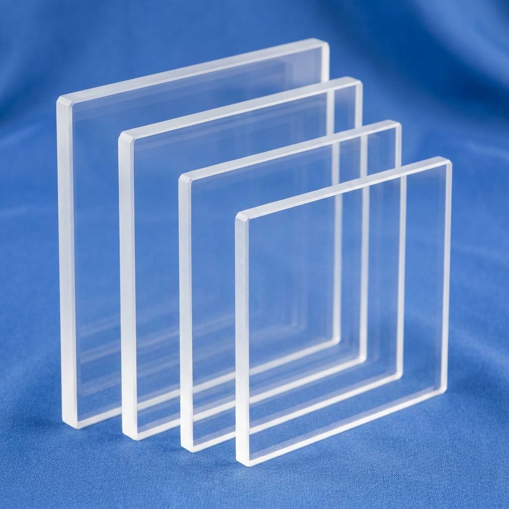
Laser Cut Quartz Glass Plate Fused Silica Precision Custom Size
CNC laser profile profiling, micro-crack-free beveling, dimensional tolerances down to ±0.05 mm for customized instrumentation.
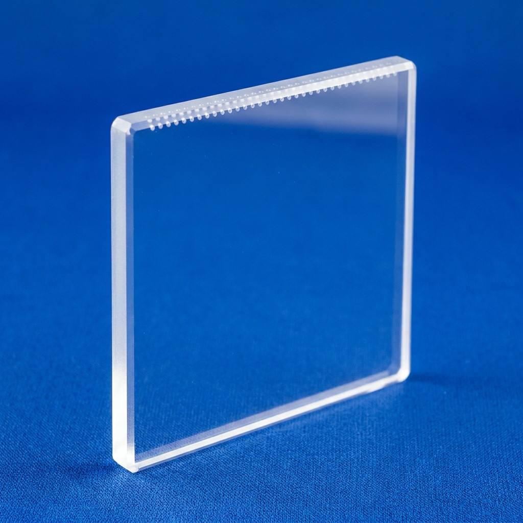
Quartz Optical Flat Plate Fused Silica High Flatness Polished Custom
Double-sided super-polishing with surface flatness λ/10 to λ/20 @ 632.8 nm; Ra < 0.5 nm for interferometer and laser mirror substrates.

Semiconductor Quartz Plate Fused Silica Substrate High Purity Custom
Ultra-pure synthetic fused silica with total metallic trace ≤20 ppm; high dielectric breakdown strength for silicon wafer carrier applications.

Slotted Quartz Plate Grooved Fused Silica Sheet Precision Custom Size
Micro-milled comb slots and custom grooves designed for vertical LPCVD/PECVD batch wafer processing boats and chemical immersion racks.
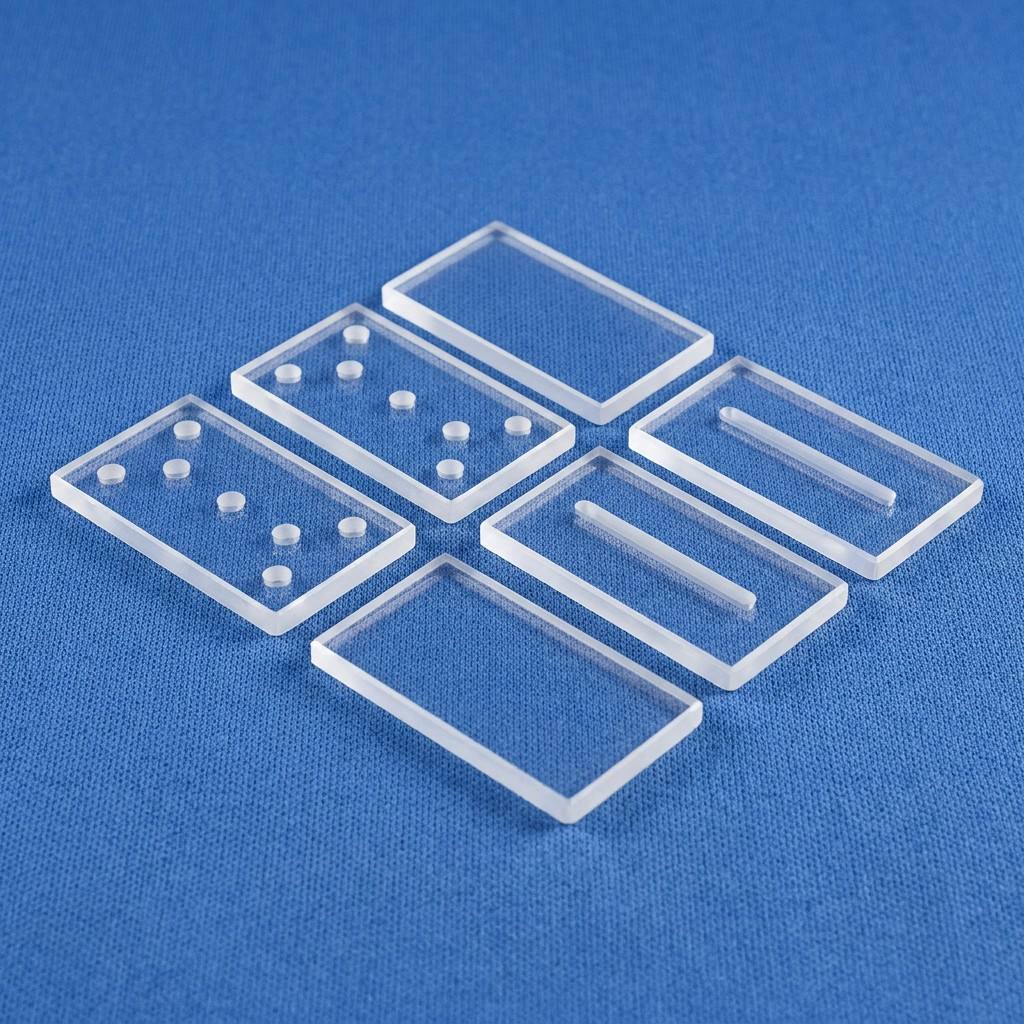
Quartz Glass Sheet 10mm 20mm 30mm Thick Fused Silica Heat Resistant
Heavy-gauge block-sawn thermal protection sheets capable of continuous 1100 °C service and extreme 1200 °C rapid thermal annealing cycles.

Round Quartz Plate Disc Fused Silica Clear Polished Custom Diameter
Round discs from Ø10 mm to Ø600 mm, ground C-edges, bubble-free class 0/1 compliance for inspection viewports and laser debris shields.
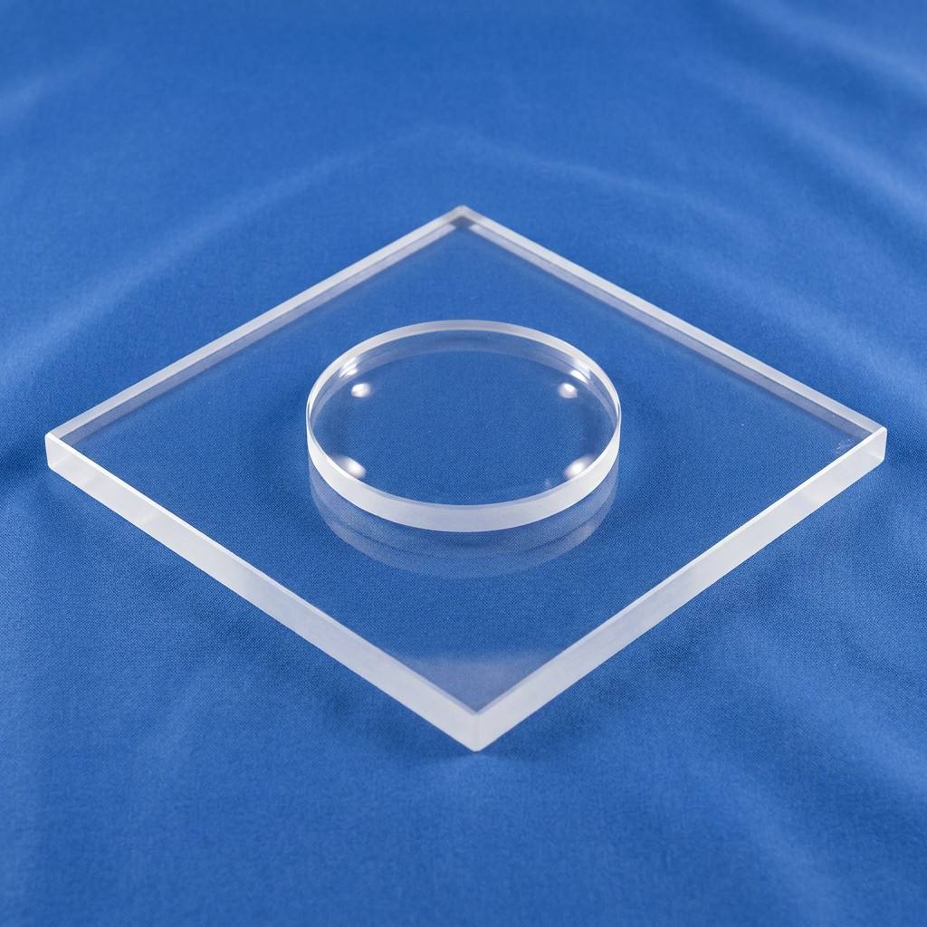
Quartz Glass Plate for Optical Window Fused Silica High Transmittance
Deep-UV JGS1 optical transmission exceeding 90% at 185–260 nm; laser scratch-dig 20/10 for spectroscopy and laser beam steering heads.
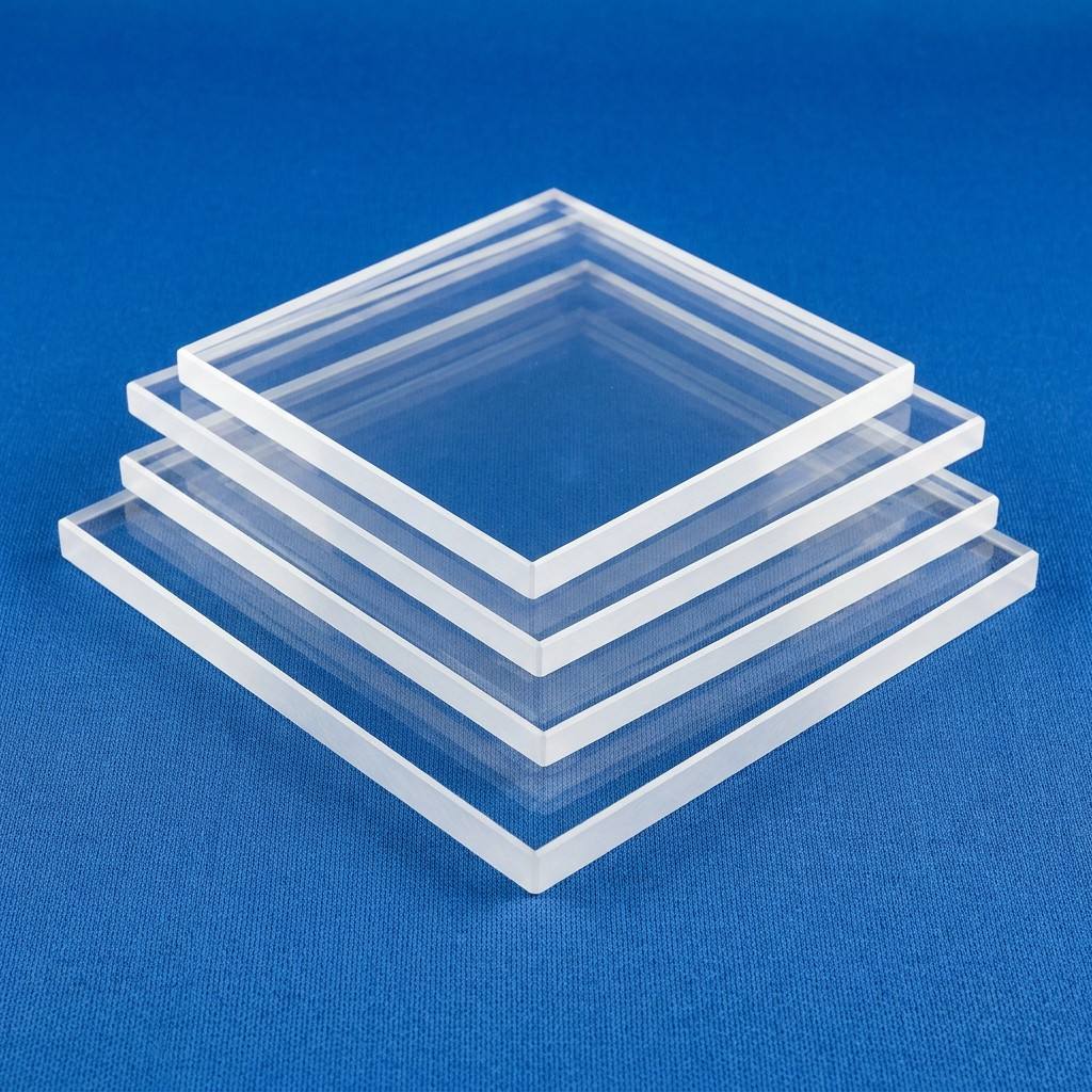
Quartz Plate with Center Hole Fused Silica Clear Polished Custom Size
Ultrasonic and CNC waterjet hole trepanning; zero edge-chipping for electrode pass-through flanges, sensors, and vacuum deposition stages.
White Paper: Sourcing High-Purity Fused Quartz Substrates for Berlin's High-Tech Ecosystem
As the European Union intensifies its strategic investments in sovereign semiconductor architectures, quantum computing infrastructure, and photonic quantum technologies, Berlin has solidified its position as Germany's foremost research and deep-tech commercialization nexus. From the research institutes anchored within Berlin-Adlershof (WISTA)—such as the Ferdinand-Braun-Institut (FBH) and the Max Born Institute—to semiconductor manufacturing corridors across Berlin-Brandenburg, procurement engineers and principal optical physicists face rigorous requirements when sourcing fused quartz and synthetic fused silica glass substrates.
The selection of an industrial quartz glass substrate supplier requires uncompromising quality assurance protocols, verifiable thermal-mechanical consistency, and deep metallurgical clarity regarding raw silica sand source origins. Headquartered in Donghai County, Jiangsu Province—globally acknowledged as China's Quartz Capital—VEZLO Quartz operates a continuous 33,000 m² production footprint dedicated to melting, precision slicing, super-polishing, and ultrasonic CNC profiling of fused silica flatware. This technical dossier establishes an engineering framework for evaluating quartz substrate grades, localized integration contexts in the Berlin metropolitan area, and international procurement risk-mitigation strategies.
Information Gain Criterion: Unlike commodity float glass or borosilicate alternatives (e.g., Borofloat® 33), fused quartz provides an extraordinary near-zero coefficient of thermal expansion (5.5 × 10⁻⁷/°C), allowing zero optical phase distortion across severe thermal gradients up to 1100 °C. Our direct Chinese supply route cuts sub-tier distributor markups while ensuring direct material batch traceability via GD-MS (Glow Discharge Mass Spectrometry) assays.
Material Cross-Reference & Physical Property Thresholds
Optical engineers in Berlin commonly reference German DIN ISO 10110 standards alongside European cross-industry designations. VEZLO Quartz produces substrates classified across JGS1 (Synthetic Fused Silica, deep UV optimized), JGS2 (Fused Quartz melted from natural crystal, UV-VIS transparent), and JGS3 (Infrared Fused Quartz melted via vacuum heating, hydroxyl-free < 2 ppm OH⁻). The performance delta across optical, thermal, and mechanical parameters is summarized in the verified engineering matrix below:
| Physical / Chemical Property | JGS1 (Synthetic Deep-UV) | JGS2 (Optical Fused Quartz) | JGS3 (Low-OH Infrared Grade) | DIN / International Standard |
|---|---|---|---|---|
| Optical Transmission Band | 185 nm – 2500 nm (>90% @ DUV) | 220 nm – 2500 nm | 260 nm – 3500 nm (No OH Absorption) | DIN 58925-1 Spectrophotometry |
| Hydroxyl Content ([OH⁻]) | ≈ 1200 ppm | ≈ 150 – 200 ppm | ≤ 2 – 5 ppm | FTIR Infrared Spectroscopy |
| Thermal Expansion (0–300 °C) | 5.4 × 10⁻⁷ / K | 5.5 × 10⁻⁷ / K | 5.5 × 10⁻⁷ / K | DIN 51045 Dilatometry |
| Softening / Annealing Point | 1730 °C / 1180 °C | 1683 °C / 1215 °C | 1700 °C / 1220 °C | ASTM C338 / ISO 7884-2 |
| Refractive Index (nd @ 589.3 nm) | 1.4585 | 1.4585 | 1.4585 | Abbe Refractometry ±0.0001 |
| Surface Roughness (Super-polished) | Ra ≤ 0.3 nm (Sub-Angstrom) | Ra ≤ 0.5 nm | Ra ≤ 0.8 nm | White Light Interferometry (WLI) |
| Internal Bubble Quality | DIN ISO 10110-3: 1/0; B0 | DIN ISO 10110-3: 1/1×0.1 | DIN ISO 10110-3: 1/2×0.16 | Polariscopic Laser Darkfield |
Berlin Regional Applications: Where High-Purity Quartz Drives Innovation
The industrial landscape of Berlin-Brandenburg is defined by high-value, specialized technology enclaves requiring custom non-standard quartz glass substrates rather than bulk consumer glass:
Berlin-Adlershof Photonics Hub
Super-polished fused silica optical flats act as primary mirror carriers, laser window ports, and beam dump splitters in diode laser modules, ultrafast fiber laser amplifiers, and quantum communication transceivers.
Silicon & GaN Semiconductor Fabs
Micro-slotted quartz support plates and ultra-pure wafers serve as batch carriers for thermal oxidation, chemical vapor deposition (CVD), and wafer thinning temporary bond substrates across local Brandenburg cleanrooms.
Biomedical & Microfluidic Labs
Laser-trepanned fused silica plates with custom micro-channels support fluorescence microscopy, sequencing flow cells, and automated immunoassays without autofluorescence interference in life science clusters.
Berlin-Brandenburg Industry Trends Shaping Material Demand
Two primary macroeconomic forces are reshaping the procurement parameters for quartz substrates in Berlin:
1. Escalation of Ultrafast UV and Deep-UV Processing: The convergence of micro-machining and excimer lasers operating at 193 nm (ArF) and 248 nm (KrF) necessitates substrates with absolute homogeneity and zero color-center formation under sustained gigawatt laser exposure. Fused quartz with low solarization characteristics and exceptional internal transmission has superseded standard borosilicates.
2. Structural Cost Realignment in German High-Tech Sourcing: Amid heightened regional energy tariffs across Germany, local processing of raw quartz blocks has experienced severe inflationary pressure. Engineering firms in Berlin are increasingly opting for primary Chinese synthesis and initial rough/precision processing, followed by dedicated air-cargo drop shipments directly into Berlin Brandenburg Airport (BER). By maintaining an unbroken internal supply chain from high-purity quartz sand refine (≤20 ppm trace metals) to CNC cold-working, VEZLO Quartz provides Berlin enterprises with competitive pricing advantages without compromising DIN ISO dimensional or surface specifications.
Why Berlin Procurement Teams Partner with VEZLO Quartz
Combining China's primary raw quartz mineral basin with state-backed scientific R&D and verified export trade security.
Donghai Mineral Origin
Situated within China's Quartz Capital with 50-mu production grounds. We purify our own high-purity quartz sand (≤20 ppm metals) across 13 proprietary grades, eliminating raw material stockout risks.
State-Recognized R&D
Developer of the 320 mm provincial science-supported semiconductor tube and newly reviewed 520 mm large-diameter furnace components, investing > RMB 5 million annually in advanced silica engineering.
Export Protection & Trade Assurance
Onsite Alibaba-verified facilities, zero-risk payment mechanisms, ISO-compliant packaging using anti-static vacuum packs and shock-damped export wooden crates for sea, rail, or air routes to Germany.
2-Hour Rapid Response & 50% Reorder
English- and German-compatible technical sales desk providing engineering reviews within 2 hours. Over 50% repeat order retention from international buyers confirms long-term metallurgical consistency.
Frequently Asked Questions for Berlin Engineers
Direct technical answers addressing German customs clearance, optical metrology, tolerances, and logistics.
How do you ensure optical substrates comply with DIN ISO 10110?
Every polished optical plate and disc undergoes laser Fizeau interferometry (flatness measurement down to λ/20) and optical darkfield inspection for bubbles and inclusions per DIN ISO 10110-3. Inspection certificates detailing transmission, surface roughness (Zygo profilometry), and dimensional accuracy are provided with each export crate.
What are the shipping transit times and logistics channels to Berlin?
For urgent R&D prototyping in Berlin-Adlershof, we utilize express airfreight (DHL Express / FedEx Priority / Air Cargo to Berlin Brandenburg Airport BER) with typical transit of 4 to 7 business days. For volume semiconductor wafer production runs, multimodal maritime shipments via Hamburg Port combined with Deutsche Bahn rail freight offer optimal freight economics.
How are fragile quartz glass sheets packed against transit damage?
Substrates are individually cleaned in an ultrasonic DI-water bath, sealed in vacuum-free antistatic bags or cleanroom polymer cassettes, interleaved with non-abrasive optical tissue, encapsulated in multi-layer high-density EPE pearl cotton, and bolted into reinforced, fumigation-free ISPM-15 compliant plywood cases equipped with Tip-N-Tell shock indicator tags.
What German customs (Zoll) and import requirements apply?
Quartz glass plates are classified under HS Code 7002.31 / 7002.39 / 7006.00 (fused quartz/silica plates and sheets). We supply full Commercial Invoices, Packing Lists with precise Net/Gross weights, and Certificates of Origin (CO). German buyers require an active EORI number for standard ATLAS customs release; DDP (Delivered Duty Paid) terms are available upon request.
Can you manufacture custom slotted plates and center holes from CAD drawings?
Yes. Our cold processing facility is equipped with 5-axis ultrasonic CNC milling centers, diamond wire slicers, and precise CO2/UV laser machining systems. We accept STEP, DWG, DXF, or PDF engineering drawings to produce tight internal radii, custom step-down shoulders, and slotted comb teeth with tolerances up to ±0.02 mm without micro-fracturing.
What is the minimum order quantity (MOQ) for custom prototypes?
We actively support academic research laboratories, startup spin-offs, and industrial pilot lines across Berlin with flexible low-volume MOQs—starting from 2 to 5 pieces for custom geometry prototypes. Volume pricing discounts automatically apply as batches transition to full recurring production runs.
Connect with VEZLO Quartz Engineering Support
Require custom optical tolerances, high-transmission DUV synthetic silica, or thermal carrier plates for your Berlin manufacturing facility? Send your technical drawings or specification parameters to our application engineering team today for an authoritative feasibility review and competitive commercial offer within 2 hours.