Featured Semiconductor Fused Silica & Quartz Components
Direct-from-source precision fused silica products manufactured in Donghai, certified to rigid dimensional, optical, and thermal tolerances for front-end wafer fabrication.


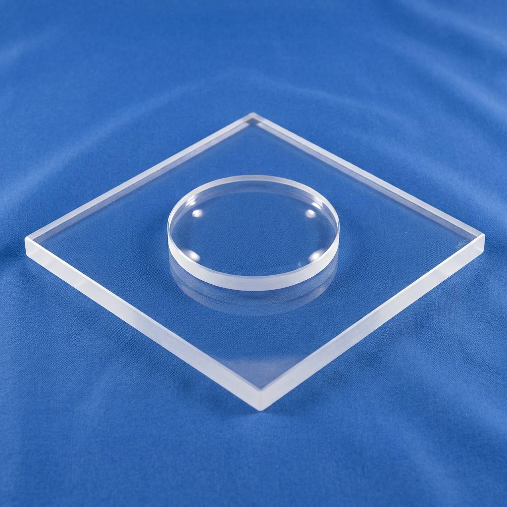
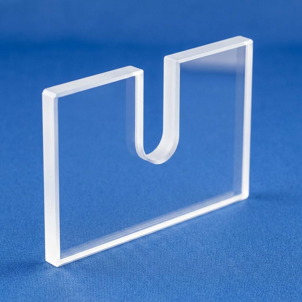
Engineering Strategic Supply Lines: China Wholesale Quartz Crucibles in Fukuoka
The island of Kyushu, historically crowned Japan's "Silicon Island," is experiencing a modern semiconductor renaissance. Centered around major logistics and trade gateways in Fukuoka, the prefecture acts as the primary engineering, distribution, and transactional hub linking international material refineries with high-density fabrication plants across Kumamoto, Nagasaki, and Oita. In this microelectronics landscape, raw material purity governs wafer throughput. The demand for industrial semiconductor-grade quartz crucibles, high-temperature diffusion tubes, and fused silica consumable spare parts has scaled exponentially.
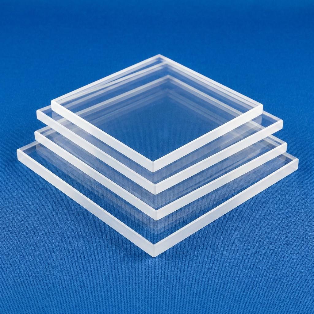
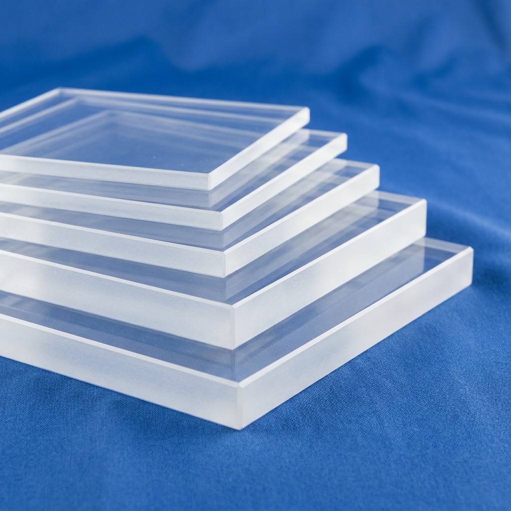
VEZLO Quartz operates as an integrated manufacturer and direct wholesale partner, providing high-purity fused quartz components to engineering departments, original equipment manufacturers (OEMs), and high-volume wafer foundries operating within Fukuoka's commercial sphere. Operating from our manufacturing base in Donghai County—globally recognized as China’s quartz crystal capital—we fuse local raw natural quartz with synthetic deposition methods. The resulting crucibles, tubes, and optical window plates withstand the operational pressures of modern Czochralski (CZ) crystal pulling, horizontal and vertical diffusion, dry plasma etching, and chemical vapor deposition (CVD).
Crucible & Fused Silica Material Characteristics
Semiconductor manufacturing demands materials that bridge absolute thermal shock resistance with chemical inertness. Fused silica quartz engineered at VEZLO delivers a near-zero coefficient of thermal expansion (5.5 × 10⁻⁷ /°C), allowing quartz furnace components and crucible bodies to transition through rapid thermal processing (RTP) without thermal fatigue, micro-cracking, or structural warping.
| Material Metric | High-Purity Natural Quartz | Synthetic Fused Silica | Impact on Semiconductor Yield |
|---|---|---|---|
| SiO₂ Purity Level | ≥ 99.995% | ≥ 99.9999% (6N) | Mitigates heavy-metal lattice poisoning in silicon ingots |
| Hydroxyl (OH⁻) Content | < 30 ppm (Dry Melt) | < 1 ppm to 1,200 ppm (Configurable) | Controls structural viscosity and prevents sag at >1200°C |
| Softening Point | ≈ 1,683 °C | ≈ 1,600 °C | Guarantees dimensional stability in CZ pullers and LPCVD |
| Total Metallic Impurities | ≤ 15–20 ppm | ≤ 0.1 ppm | Eliminates copper, iron, and sodium drift into active gate zones |
| Thermal Shock Resistance | 1,100°C into cold water quench | 1,150°C rapid cycle resilient | Eliminates catastrophe during furnace tube loading operations |
Localized Industrial Applications Across Fukuoka and the Kyushu Corridor
Procurement teams based in Fukuoka service a multifaceted semiconductor and precision manufacturing ecosystem across northern and central Kyushu. Fused quartz products serve unique thermal, chemical, and optical roles across several micro-sectors:
Czochralski (CZ) Ingot Pulling
Fabrication plants require single-use, large-diameter quartz crucibles ranging from 18 to 36 inches to pull monocrystalline silicon ingots. Low-bubble natural quartz exterior layers provide heat retention, while ultra-pure synthetic inner layers resist degradation from molten silicon.
Diffusion & Oxidation Tubes
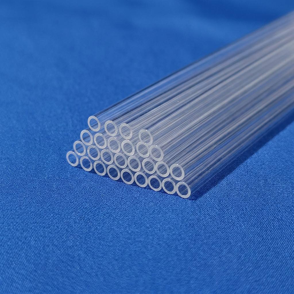
Thermal processing furnaces require our 2 mm to 500 mm OD clear quartz tubes. Highly uniform wall thicknesses prevent temperature variations, which protects wafer runs from uneven dopant diffusion and thermal slip lines.
Wet-Bench Etching Tanks
Front-end cleaning lines rely on custom-welded quartz baths and tanks. Fused silica offers resistance to harsh acids (including hot sulfuric peroxide and nitric blends), preventing vessel leaching and surface erosion during wafer batch cleans.
Compound Semiconductor (SiC/GaN) Processing
With Kyushu emerging as a hub for electric vehicle power electronics, SiC epitaxial growth and gallium nitride (GaN) processing demand custom-engineered quartz boats, shields, and high-pressure viewing discs capable of handling high-temperature reactive chemistries.
Plasma Etch Chamber Rings
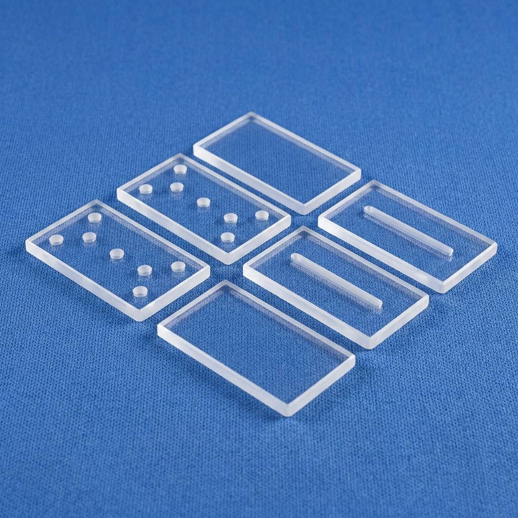
High-density plasma etching requires dimensionally precise quartz focus rings, showerheads, and clamp rings. Our precision CNC grinding and beveled-edge polishing mitigate micro-chipping, ensuring uniform RF coupling and lower defect density.
Fukuoka Semiconductor Supply Chain Trends
The microelectronics manufacturing strategy in Fukuoka is marked by three primary transitions:
1. Near-Source Redundancy: Kyushu fab operators are actively diversifying beyond legacy single-source regional suppliers to stabilize raw material procurement. Direct-from-factory partnerships with Chinese producers located along the Yellow Sea logistics rim provide reliable supply resilience. Shipping routes from Lianyungang/Qingdao ports to Hakata Port (Fukuoka) reduce transit times to under 48–72 hours, offering ocean transit speeds that rival domestic ground logistics.
2. Transition to Larger Ingot Diameters: Driven by automotive power electronics and 300 mm wafer expansions across Kumamoto, crucible specifications are shifting toward 28-inch, 32-inch, and larger diameters. Larger crucibles must maintain rigid wall uniformity and structural viscosity at 1,400°C+ over runs lasting more than 100 continuous hours without devitrifying.
3. Low Hydroxyl Control for Plasma Longevity: Modern dry halogen etch processes erode structural quartzware rapidly. Japanese engineering facilities prioritize lower-OH quartz formulations (<5 ppm OH) for chamber hardware, which exhibit lower erosion rates under fluorocarbon plasma chemistry and lengthen intervals between scheduled maintenance cycles.
VEZLO Manufacturing Advantages for Japanese Industrial Partners
VEZLO Quartz integrates primary material refining with precision CNC cold processing and artisanal thermal flame-working. Our technical baseline reflects decades of specialized processing:
Raw Material Ownership
Situated in Donghai County (China’s quartz capital), we control high-purity quartz sand supplies across 13 distinct grades, keeping metallic impurity levels consistently below 20 ppm total conventional metals.
Provincial R&D Recognition
Our 320 mm high-purity quartz tube was recognized as a Jiangsu Provincial Science & Technology Support Project, while our 520 mm large-diameter furnace tube completed national reviews for high-end microelectronics equipment.
Full-Spec Custom Fabrication
From complex welded wafer carriers, boats, and cleaning tanks to ground optical viewport discs, our workshop manufactures directly against CAD/STEP drawings with standard tolerances down to ±0.05 mm.
Cleanroom Packaged Export
Fragile quartzware is ultrasonically cleaned, double vacuum-bagged in cleanroom enclosures, and packaged within reinforced, shock-absorbing export crates to ensure pristine condition upon arrival at Hakata Port or Fukuoka Airport.
Frequently Asked Questions: Sourcing Quartz Crucibles & Glassware in Fukuoka
What is the lead time for standard vs. custom quartz crucibles shipped to Fukuoka?
How does VEZLO Quartz prevent devitrification (crystallization) during high-temperature runs?
Can you manufacture semiconductor quartzware precisely to custom Japanese CAD drawings?
What documentation and batch quality certifications are provided for cleanroom intake?
How are delicate, high-aspect-ratio quartz tubes and crucibles protected against shipping fracture?
Connect with Our Semiconductor Quartz Engineering Team
Accelerate your Fukuoka procurement pipeline. Submit your technical drawings or specification parameters to receive an engineering review, trace impurity data sheets, and competitive wholesale quotes within 2 hours.
Send an Inquiry