Precision Quartz Plates & Core Components
Manufactured from ultra-pure natural quartz crystal and synthetic silicon precursors. Surface flatness up to λ/10, scratch-dig 20-10, with operational stability exceeding 1,100°C.

Semiconductor Quartz Plate Fused Silica Substrate High Purity Custom
Total metallic impurities ≤20 ppm, CMP double-side polished with Ra <0.5 nm for wafer carriers, lithography masks, and sub-micron semiconductor processes.
Contact Us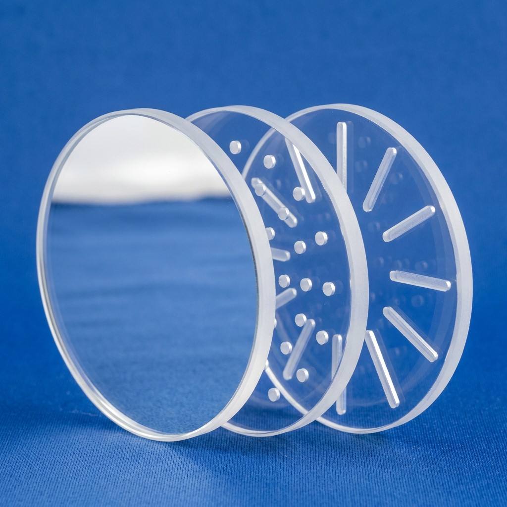
Rectangular Quartz Plate Fused Silica Clear Precision Cut Custom Size
Custom CNC diamond edge chamfering, laser-cut profiling, dimensional tolerance within ±0.05 mm, optimal for UV curing windows and inline sight glass.
Contact Us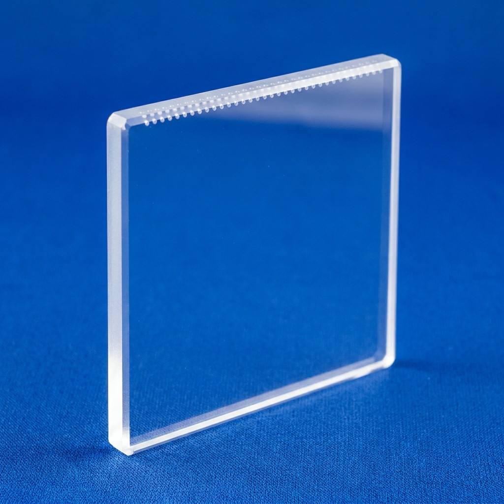
Quartz Optical Flat Plate Fused Silica High Flatness Polished Custom
Optical reference flats with surface figure λ/10 to λ/20 at 632.8 nm, parallelism <5 arcsec, engineered for laser interferometry and optical inspection stages.
Contact Us
Quartz Tube for Ozone Generator High Purity Fused Silica Ozone Free
Precision titanium-doped fused quartz engineered to cut 185 nm line emissions while transmitting 254 nm germicidal radiation for water and cleanroom treatment systems.
Contact Us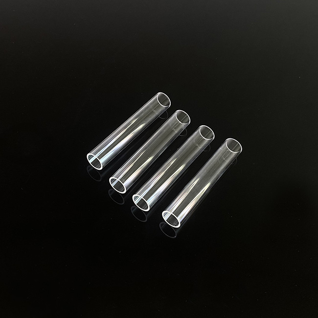
Large Diameter Clear Quartz Borosilicate Glass Tube round Fused Silica
Outer diameter capacity up to 520 mm with uniform wall control, formulated for high-vacuum diffusion chambers, CVD process reaction tubes, and torch welding.
Contact Us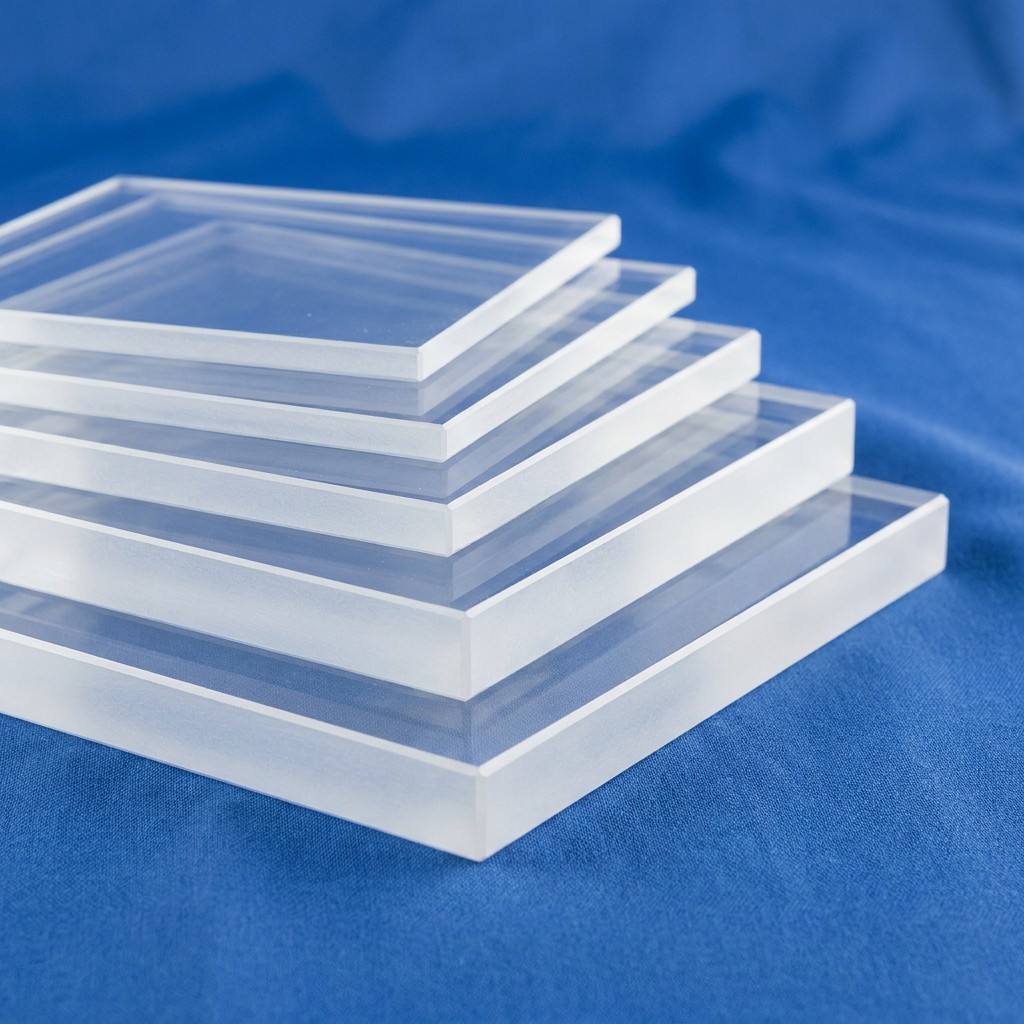
Quartz Fireplace Viewing Glass Plate Heat Resistant Fused Silica
Withstands thermal gradients from 1,100°C to cold liquid immersion without cracking; thermal expansion coefficient 5.5 × 10⁻⁷ /°C for industrial kiln viewing.
Contact Us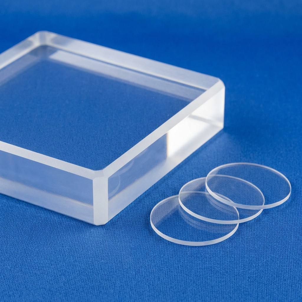
Quartz Plate for Laboratory Fused Silica Clear Heat Resistant Custom
Chemical inertness to severe acids (except HF), high UV transmission in the 200–400 nm band, custom slotted for spectrometry and analytical biochemistry apparatus.
Contact Us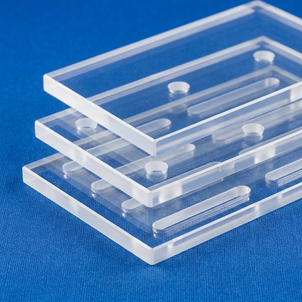
Quartz Disc with Groove Fused Silica Plate Clear Polished Custom Size
Micro-machined sealing grooves, step-boring, and o-ring recesses CNC ground into high-flatness discs for vacuum flange observation and laser chamber enclosures.
Contact UsFused Silica vs. Natural Fused Quartz: Optical Grade Classifications
A rigorous comparative analysis for optical designers, process integration engineers, and procurement managers in the Greater Kuala Lumpur high-technology corridor.
Selecting the appropriate amorphous silica substrate requires a thorough understanding of deep ultraviolet (DUV) spectral cutoff points, hydroxyl (OH⁻) absorption bands in the near-infrared (NIR), and micro-bubble classifications. In high-precision optoelectronic devices and laser cutting assembly plants across Selangor and Kuala Lumpur, material failure frequently traces back to thermal-stress devitrification or photochemical solarization caused by selecting improper quartz glass grades.
| Grade Category | Material Precursor | Transmission Band | Typical OH Content | Primary Industrial Use-Case |
|---|---|---|---|---|
| JGS1 (Synthetic Silica) | High-purity SiCl₄ chemical synthesis | 185 nm – 2,500 nm (DUV / UV) | < 1,200 ppm (or <10 ppm for low-OH) | Excimer laser optics, semiconductor lithography masks, UV spectrophotometry |
| JGS2 (Optical Fused Quartz) | Refined natural crystal melting (H₂/O₂) | 220 nm – 2,500 nm (Visible / VIS) | < 150 – 200 ppm | Optical sight glasses, high-pressure discharge lamps, analytical instrument stages |
| JGS3 (Infrared Fused Silica) | Electrically melted natural crystal | 260 nm – 3,500 nm (NIR / IR) | < 5 ppm (Water-free) | CO₂ laser windows, thermal imaging viewports, pyrometric furnace observation |
| Semiconductor Clear Tube | High-purity Donghai quartz sand | 280 nm – 2,500 nm (Thermal) | < 30 ppm | Diffusion furnace liners, LPCVD process reactors, thermal oxidation carriers |
Precision Quartz Applications in the Greater KL Industrial Ecosystem
Serving advanced assembly, test, and photonics facilities across Shah Alam, Petaling Jaya, Cyberjaya, Bangi, and the broader Selangor industrial landscape.
Semiconductor OSAT & Advanced Packaging
Malaysia accounts for approximately 13% of the world's backend semiconductor assembly and testing. In the automated packaging corridors of Klang Valley and Petaling Jaya, our ultra-flat quartz plates act as rigid, transparent wafer carriers for temporary bonding and de-bonding (TBDB) workflows, laser lift-off (LLO) carrier substrates, and chemical-mechanical planarization (CMP) conditioning retainers.
Wafer Support • Thin-Die CarriersIndustrial Laser Cutting & Photonics Machinery
The manufacturing belts of Shah Alam and Subang rely heavily on multi-kilowatt fiber and UV solid-state laser cutting equipment for sheet metal, precision electronics, and medical device fabrication. Our anti-reflective (AR) coated fused silica debris shields and protective laser windows feature high bulk laser damage thresholds (>10 J/cm² at 1064 nm, 10 ns) to safeguard sensitive focusing optics from molten spatter and thermal distortion.
Laser Windows • AR ShieldingUniversity & Public Research Metrology
Kuala Lumpur hosts premier academic and national scientific hubs, including Universiti Malaya (UM), Universiti Kebangsaan Malaysia (UKM), and SIRIM Berhad. We supply custom quartz optical flats, UV spectroscopy micro-cuvettes, and vacuum reaction chambers with ground quartz joints for cutting-edge investigations in nanotechnology, green energy catalysts, and microfluidics.
SIRIM Standards • High-Vacuum FlangesEmerging Trends Driving Optical Quartz Demand in Malaysia
Aligning with the National Semiconductor Strategy (NSS) and the New Industrial Master Plan (NIMP 2030).
Shift from OSAT to Front-End Wafer Fabrication
Malaysia is aggressively positioning itself to capture front-end wafer fabrication facilities and specialized compound semiconductor lines (SiC, GaN). This transition demands process quartzware of extreme chemical purity: diffusion tubes exceeding 500 mm OD, high-capacity wafer boats, and ultra-flat furnace baffles resistant to corrosive dopant atmospheres.
Front-End Semiconductor EvolutionExpansion of Solar PV & Green Energy Equipment
As Southeast Asia deepens its renewable manufacturing supply chain, solar cell and ingot manufacturing plants across Selangor and neighboring logistics hubs are upgrading to higher-efficiency n-type TOPCon and heterojunction (HJT) architectures. These plants require heavy-duty quartz crucibles and thermal quartz tubes that survive continuous runs at 1,450°C without crystalline restructuring.
Photovoltaic Thermal InfrastructureStringent Cleanroom Contamination Protocols
Modern micro-optics and medical diagnostic devices assembled in Kuala Lumpur cleanrooms require suppliers to guarantee low-outgassing, chemical residue-free, and particulate-controlled components. Fused silica has emerged as the premier replacement for borosilicate and technical ceramics due to its zero-porosity surface and zero trace metal leaching.
Zero-Outgassing PurityRapid Sourcing Integration via Port Klang & KLIA
Global supply chain diversification favors agile manufacturers who provide engineering validation, quick turnaround on customized drawings, and air-freight options into Kuala Lumpur International Airport (KLIA) or ocean consolidations through Port Klang (Westports/Northport). Real-time technical support eliminates costly downtime for local plant operators.
Direct Regional LogisticsWhy Tier-1 Engineers Source Optical Quartz from VEZLO
Combining world-class mineral deposits in Donghai with multi-axis CNC cold processing and high-temperature flame fabrication.
Raw Mineral Dominance (Donghai Cluster)
Situated within China's recognized "Quartz Capital" across a 33,000 m² operating facility, our production chain starts from ultra-pure silica deposits yielding total metal impurities ≤20 ppm across 13 proprietary sand grades. This raw material purity prevents structural micro-inclusions, striae, and seed bubbles at the source.
≤20 ppm Metallic PurityNational & Provincial Science Recognition
Our 320 mm high-purity quartz tube for ultra-large-scale integrated circuit processing was selected as a prestigious Jiangsu Provincial Science & Technology Support Project. Furthermore, our 520 mm large-diameter tube passed national new product reviews, proving our technological standing in 12-inch and 14-inch wafer furnace components.
Provincial Science Award WinnerFull-Spectrum CNC Cold & Hot Processing
We do not simply draw standard shapes; we machine high-complexity components to drawing. Capabilities include ultrasonic micro-drilling, surface double-sided planetary polishing (CMP), CNC step milling, edge profiling, slotting, precision optical coating, and artisan lathe torch welding of custom quartz instruments.
Complex Custom FabricationMetrology-Backed Quality Assurance
Every optical plate and substrate order is verified with laser interferometers (Zygo), spectrophotometers measuring transmission from 190 nm to 3,200 nm, coordinate measuring machines (CMM), and optical polariscopes to verify stress birefringence ≤5 nm/cm, ensuring absolute compliance before packing.
Zygo Verified FlatnessEngineered Cleanroom Packaging
Fragile optical elements are cleaned via multi-stage ultrasonic deionized water cascades, vacuum-sealed in static-shielding film inside Class 100/1000 cleanrooms, and packed into shock-absorbing, multi-layer pearl cotton cases with integrated tilt/drop indicators for international export safety.
Zero-Chipping Transit GuaranteeDirect Engineering Consultation
No non-technical intermediaries. Technical inquiries from Kuala Lumpur, Bayan Lepas, or Johor are evaluated directly by materials scientists and optical production technicians, providing initial feasibility checks and DFM (Design for Manufacturability) advice within 2 hours.
≤2 Hour Rapid AssessmentFrequently Asked Questions by Malaysian Sourcing & Engineering Teams
Key technical, commercial, and logistics considerations for importing optical quartz plates and custom parts into Kuala Lumpur and Selangor.
What are the lead times and shipping routes for custom optical quartz plates to Kuala Lumpur?
How do you ensure optical quartz surfaces do not degrade in Malaysia's tropical humidity during storage?
What documentation and certifications are supplied with semiconductor-grade quartzware?
What HS codes and tax considerations apply when clearing quartz plates through Royal Malaysian Customs?
Can you manufacture custom quartz parts directly from CAD drawings (STEP, DXF, DWG)?
What is the difference in operational lifetime between fused quartz and synthetic silica in UV curing lines?
Request a Technical Quotation for Your Quartz Project
Consult with our quartz engineering specialists. Send your technical drawings, dimensional tolerances, and operating specifications for an immediate feasibility evaluation and formal quotation within 2 hours.