
Quartz Photomask Substrate Plate Fused Silica UV Grade Ultra Thin
Engineered for extreme deep-UV transmission down to 193 nm. Features ultra-flat parallelism (λ/4 per 100mm) and minimal bubble inclusions for photolithography masking.
Inquire NowPrecision-machined fused silica sheets engineered to meet rigorous DIN, ISO, and SEMI standards for regional microelectronics, laser manufacturing, and laboratory testing facilities across Lower Silesia.
Engineered for extreme deep-UV transmission down to 193 nm. Features ultra-flat parallelism (λ/4 per 100mm) and minimal bubble inclusions for photolithography masking.
Inquire Now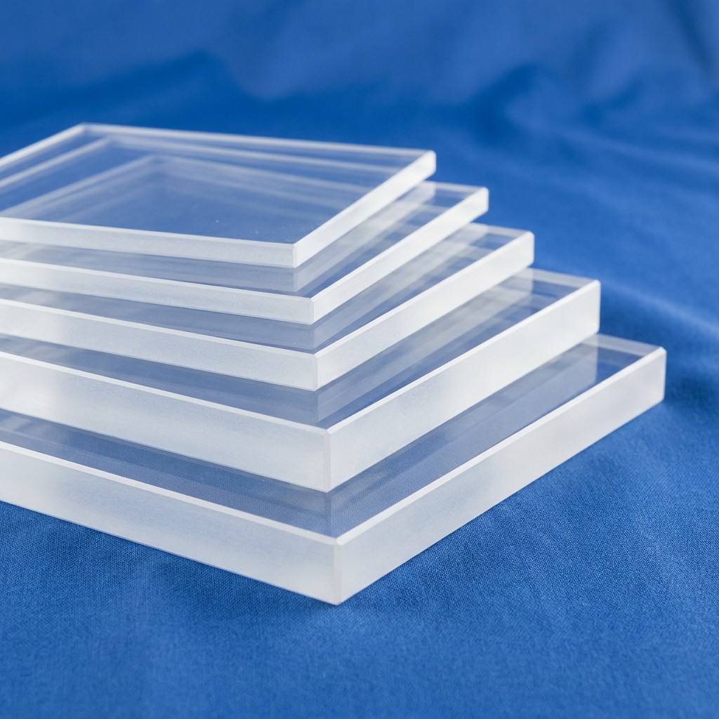
Near-zero thermal expansion coefficient (5.5 × 10⁻⁷/°C) offering superior resistance to thermal shock up to 1,200°C without mechanical failure or structural clouding.
Inquire Now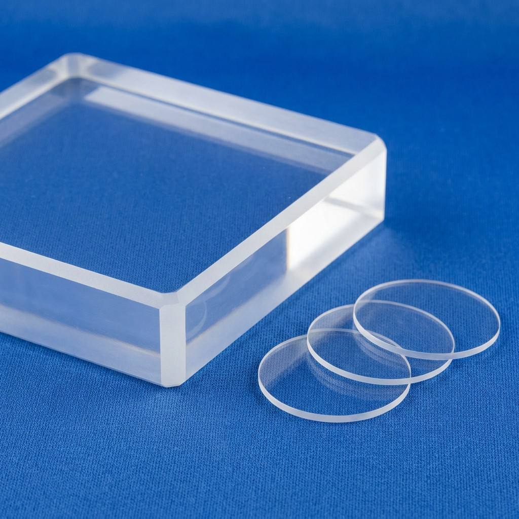
Exceptional chemical inertness against concentrated acids and corrosive reagents (except HF). Perfectly suited for digestion baths, analytical fixtures, and petri substrates.
Inquire Now
Electronic-grade double-side polished wafer carrier with total trace metal contamination strictly controlled under 20 ppm. Surface roughness achievable to Ra < 0.5 nm.
Inquire Now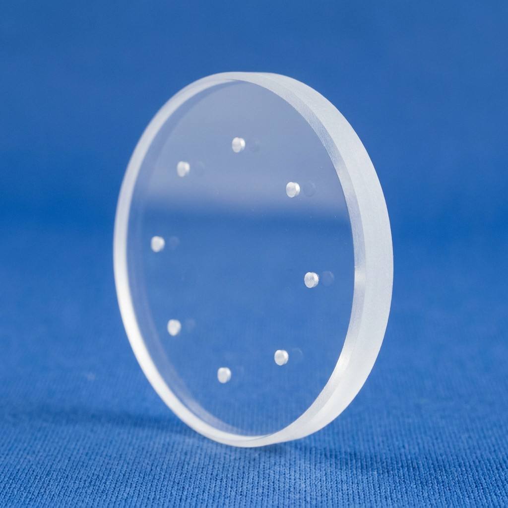
Custom 5-axis CNC diamond milled geometries, complex stepped profiles, micro-hole drilling, beveling, and laser-notched edge processing tailored directly to your CAD files.
Inquire Now
Standardized stock thicknesses offering high transmission from 260 nm to 2,500 nm. Diamond-ground perimeter edges with scratch-dig performance conforming to MIL-PRF-13830B.
Inquire Now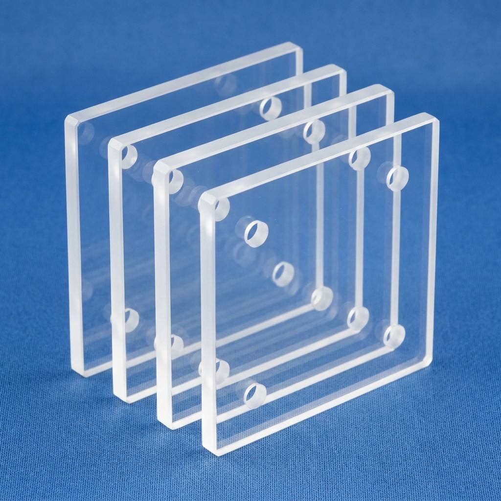
High laser-induced damage threshold (LIDT) protection shields designed specifically for multi-kilowatt fiber and industrial UV laser cutting systems common in automotive automation.
Inquire Now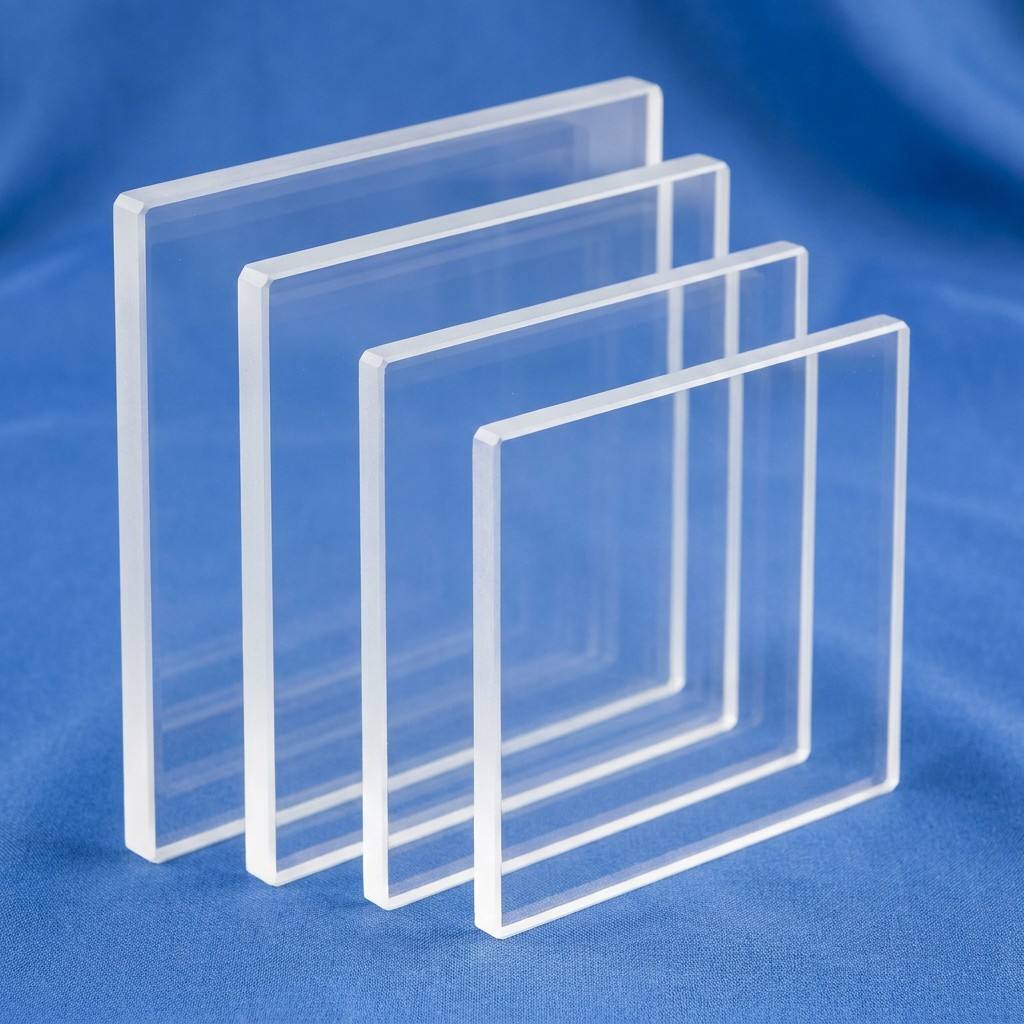
CO₂ and picosecond laser-cut customized shapes featuring chip-free margins, pristine flame-polished edges, and tight tolerance dimensions within ±0.05 mm.
Inquire NowAs southwestern Poland solidifies its role as the premier technology cluster—anchored by the Wrocław Technology Park (WPT) and neighboring Special Economic Zones—custom quartz sheet components provide vital infrastructure across four key sectors.
With massive supply chain developments including mega-scale assembly and test facilities near Miękinia and Wrocław, regional demand for electronic-grade quartzware has multiplied. High-purity quartz plates and masking substrates serve as critical tooling components in wafer carriers, furnace baffles, cleanroom inspection windows, and etching chambers requiring total chemical neutrality and trace-metal impurity budgets under 20 ppm.
Wrocław's dense ecosystem of laser integrators and photonics laboratories (closely linked to Wrocław University of Science and Technology) demands optical-grade fused silica plates. Our UV-grade sheets are deployed as high-damage-threshold (LIDT) debris shields, beam splitters, and output windows in CNC laser cutting machines and optical transceivers, resisting micro-fractures under high-fluence 1064 nm and 355 nm beam regimes.
Life-science labs and contract research organizations (CROs) inside the Wrocław Technology Park rely on optical quartz sheets for spectrofluorometric flow cells, UV transparent microplates, and autoclaving viewing ports. Fused quartz ensures zero autofluorescence under analytical excitation while resisting aggressive organic solvents, nitric acid mixtures, and cyclic thermal sterilization cycles.
The automotive corridor along the A4 motorway in Lower Silesia hosts some of Europe’s largest lithium-ion battery gigafactories. Fused quartz viewing plates are incorporated into battery cell degassing channels, high-temperature thermal test chambers, and infrared drying ovens, retaining total mechanical integrity against explosive thermal changes and chemical vapor exposure.
Regional machinery builders developing vacuum sintering systems, plasma coating lines, and diffusion furnaces require bespoke quartz observation ports and insulating baffles. Fused quartz sheets maintain continuous load-bearing performance at 1,100°C without mechanical sagging, while serving as ultra-stable calibration reference flats for optical profilometry.
Procurement teams across the Lower Silesian Voivodeship are shifting away from intermediate distributors toward direct-from-factory OEM fabrication models. The acceleration of semiconductor cleanroom projects in the Wrocław metropolitan area demands direct engineering consultations, certified material origin tracing, and customizable CNC flame-working options that intermediate stockists cannot provide efficiently.
Selecting between synthetic silica (chemical vapor deposited SiCl₄) and natural fused quartz (refined crystalline quartz) determines cost-to-performance efficiency for Wrocław procurement managers:
Local high-precision industries demand rigorous surface specifications beyond standard commercial glass cutting. Components require precision ground chamfers, CNC-machined stepped shoulders, and ultrasonic core-drilled holes to prevent micro-fissure expansion during thermal cycling.
Our production facilities maintain scratch-dig standards ranging from commercial 60/40 down to precision laser optics grade 20/10, verified through laser interferometry and optical profilometers before international crate packaging.
| Material Property | Standard Value | Industrial Relevance |
|---|---|---|
| SiO₂ Purity | ≥ 99.99% | Zero wafer contamination |
| Thermal Expansion (0-300°C) | 5.5 × 10⁻⁷ /°C | Thermal shock immunity |
| Softening Point | ≈ 1,683 °C | High-temperature envelope |
| Dielectric Strength (20°C) | 25–40 kV/mm | High-voltage insulation |
| Refractive Index (nD) | 1.4585 | Predictable beam optics |
Operating from Donghai—globally recognized as the capital of high-purity quartz—we combine mineral-source advantages with advanced industrial fabrication for mission-critical quartz sheets.
With 13 standardized grades of ultra-high-purity sand yielding total conventional metal impurities ≤20 ppm, our sheets demonstrate unrivaled structural clarity, zero internal bubbles, and long-term resistance to devitrification.
Our engineering team processes CAD technical drawings, provides material compatibility feedback, and issues official commercial quotations within an average turnaround of under 2 hours, keeping your design milestones on schedule.
Backed by our provincial Science & Technology project heritage (including large-diameter 320 mm and 520 mm semiconductor quartz products), we reinvest over RMB 5 million annually into high-precision quartz processing innovations.
Each plate is cushioned with individual shock-absorbent pearl cotton layers, vacuum sealed to preserve cleanliness, and crated in fumigation-free reinforced plywood cases guaranteed for air freight or express dispatch directly to Wrocław.
Addressing the commercial, compliance, and engineering inquiries most frequently raised by purchasing engineers across southwestern Poland.
Partner directly with an established high-purity quartz sheet manufacturer. Upload your dimensional drawings, specify thermal or optical tolerance limits, and receive a factory-direct assessment within 2 hours.
Inquire Now